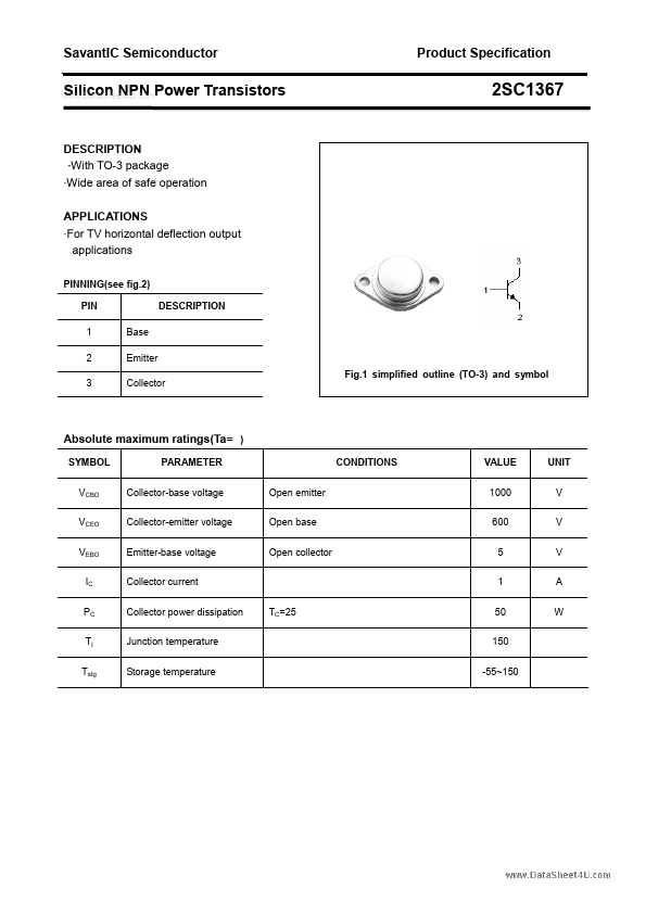
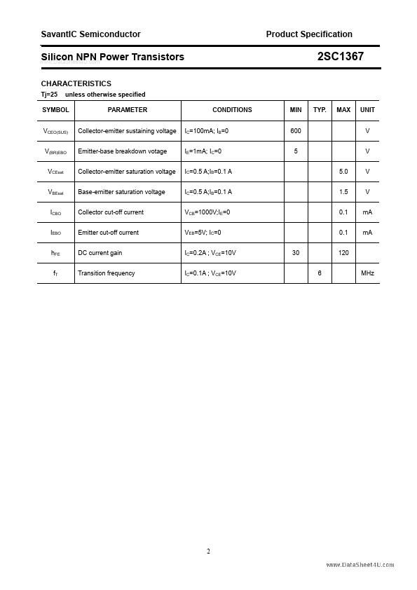
With TO-3 package
Wide area of safe operation
APPLICATIONS
For TV horizontal deflection output
applications
PINNING(see fig.2) PIN DESCRIPTION 1 Base 2 Emitter 3 Collector
Product Specification
2SC1367
Fig.1 simplified outline (TO-3) and symbol
Absolute maximum ratings(Ta= )
SYMBOL
SavantIC Semiconductor
wSwiwl.iDcatoaSnheeNt4PU.cNomPower Transistors
DESCRIPTION ·With TO-3 package ·Wide area of safe operation
APPLICATIONS ·For TV horizontal deflection output
applications
PINNING(see fig.2) PIN DESCRIPTION 1 Base 2 Emitter 3 Collector
Product Specification
2SC1367
Fig.1 simplified outline (TO-3) and symbol
Absolute maximum ratings(Ta= )
SYMBOL
PARAMETER
VCBO
Collector-base voltage
VCEO VEBO
Collector-emitter voltage Emitter-base voltage
IC Collector current
PC Collector power dissipation
Tj Junction temperature
Tstg Storage temperature
CONDITIONS Open emitter Open base Open collector
TC=25
VALUE 1000 600 5 1 50 150
-55~150
UNIT V V V A W
SavantIC Semiconductor
Silicon NPN Power Transistors
www.DataSheet4U.