Datasheet4U.com
🌙
SMG2007-C Datasheet | SeCoS Halbleitertechnologie GmbH
Part:
SMG2007-C
Description:
P-Channel MOSFET
Category:
MOSFET
Manufacturer:
SeCoS Halbleitertechnologie GmbH
Size:
635.40 KB
SMG2007-C Datasheet (PDF) Download
SeCoS Halbleitertechnologie GmbH
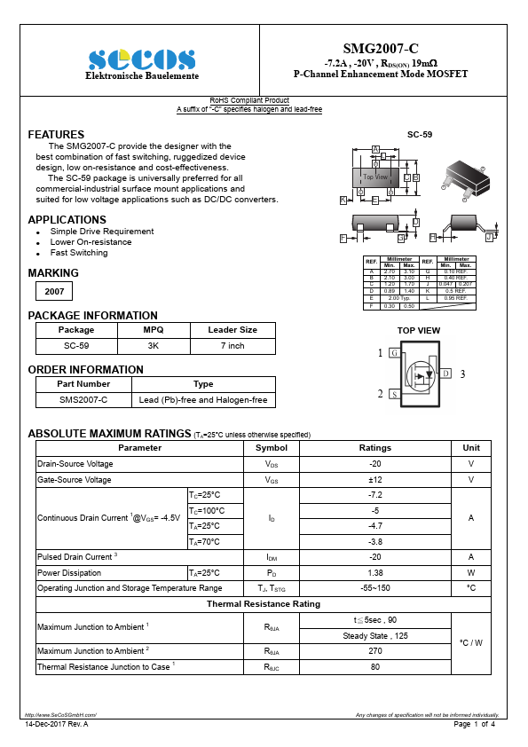
SMG2007-C
Key Features
7.2A , -20V , RDS(O ) 19mΩ P-Channel Enhancement Mode MOSFET
7.2A , -20V , RDS(O ) 19mΩ P-Channel Enhancement Mode MOSFET
×
Close