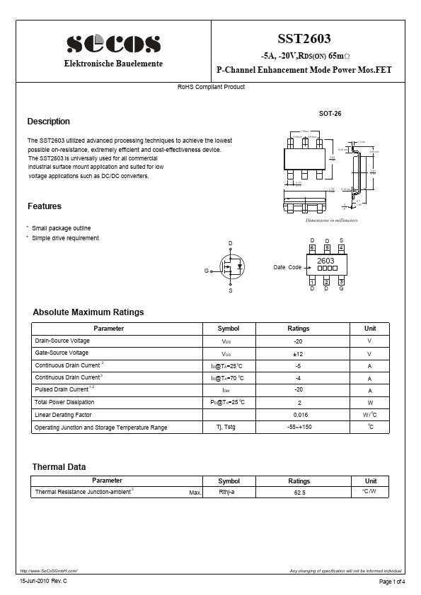
Datasheet4U Logo Datasheet4U.com

SST2603 - P-Channel MOSFET

General Description

The SST2603 utilized advanced processing techniques to achieve the lowest possible on-resistance, extremely efficient and cost-effectiveness device.

Key Features

  • Small package outline.
  • Simple drive requirement Absolute Maximum Ratings Parameter Drain-Source Voltage Gate-Source Voltage Continuous Drain Current 3 Continuous Drain Current 3 Pulsed Drain Current 1,2 Total Power Dissipation Linear Derating Factor Operating Junction and Storage Temperature Range D G S Symbol VDS VGS ID@TA=25 oC ID@TA=70 oC IDM PD@TA=25 oC Tj, Tstg SOT-26 1.90REF 0.95REF 0.95REF 0.45 REF 2.60 3.00 1.2 REF 0.60 REF 1.40 1.80 0.30 0.55 2.70 0.10 Max 3.10 o 0 0.

📥 Download Datasheet

Full PDF Text Transcription for SST2603 (Reference)

Note: Below is a high-fidelity text extraction (approx. 800 characters) for SST2603. For precise diagrams, and layout, please refer to the original PDF.

Elektronische Bauelemente SST2603 -5A, -20V,RDS(ON) 65mΩ P-Channel Enhancement Mode Power Mos.FET RoHS Compliant Product Description The SST2603 utilized advanced process...

View more extracted text
HS Compliant Product Description The SST2603 utilized advanced processing techniques to achieve the lowest possible on-resistance, extremely efficient and cost-effectiveness device. The SST2603 is universally used for all commercial industrial surface mount application and suited for low voltage applications such as DC/DC converters.