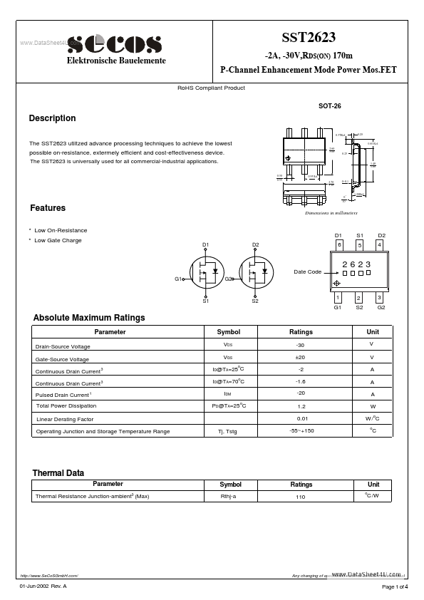
Datasheet4U Logo Datasheet4U.com

SST2623 - P-Channel MOSFET

General Description

0.37Ref.

0.20 0.60 Ref.

The SST2623 utiltzed advance processing techniques to achieve the lowest possible on-resistance, extermely efficient and cost-effectiveness device.

Key Features

  • Low On-Resistance.
  • Low Gate Charge D1 D2 Dimensions in millimeters D1 6 S1 5 D2 4 G1 G2 Date Code 2623 S1 S2 1 G1 2 S2 3 G2 Absolute Maximum Ratings Parameter Drain-Source Voltage Gate-Source Voltage Continuous Drain Current 3 Continuous Drain Current 3 Pulsed Drain Current 1 Total Power Dissipation Linear Derating Factor Operating Junction and Storage Temperature Range Tj, Tstg Symbol VDS VGS ID@TA=25 C ID@TA=70 C IDM PD@TA=25 C o o o Ratings -30 ±20 -2 -1.6 -20 1.2 0.

📥 Download Datasheet

Full PDF Text Transcription for SST2623 (Reference)

Note: Below is a high-fidelity text extraction (approx. 800 characters) for SST2623. For precise diagrams, and layout, please refer to the original PDF.

www.DataSheet4U.com SST2623 -2A, -30V,RDS(ON) 170m£[ Elektronische Bauelemente P-Channel Enhancement Mode Power Mos.FET RoHS Compliant Product SOT-26 Description 0.37Ref....

View more extracted text
Mode Power Mos.FET RoHS Compliant Product SOT-26 Description 0.37Ref. 0.20 0.60 Ref. 2.60 3.00 The SST2623 utiltzed advance processing techniques to achieve the lowest possible on-resistance, extermely efficient and cost-effectiveness device. The SST2623 is universally used for all commercial-industrial applications. 0.30 0.55 0.95 Ref. 2.70 3.10 0~0.1 0.25 1.40 1.80 0 o 10 o 1.20Ref.