S-89220A Description
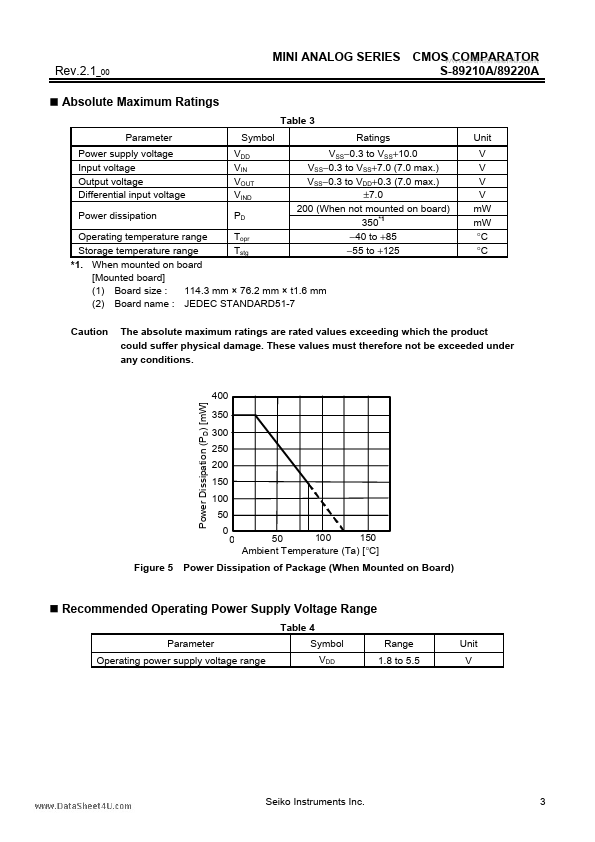
MINI ANALOG SERIES Rev.2.1_00 Ratings Table 3 Parameter Power supply voltage Input voltage Output voltage Differential input voltage Power dissipation Symbol VDD VIN VOUT VIND PD Ratings CMOS PARATOR .. S-89210A/89220A Unit V V V V mW mW °C °C Operating temperature range Topr Storage temperature range Tstg 1. When mounted on board [Mounted board] (1) Board size.
S-89220A Key Features
- Features
- Application
- Package
- Product Code List