S-89531A Description
MINI ANALOG SERIES Rev.3.1_00 0.7 μA Rail-to-Rail CMOS PARATOR S-89530A/89531A .. When mounted on board [Mounted board] (1) Board size : 114.3 mm × 76.2 mm × t1.6 mm (2) Board name.
S-89531A is MINI ANALOG SERIES 0.7 uA Rail-to-Rail CMOS COMPARATOR manufactured by Seiko Instruments.
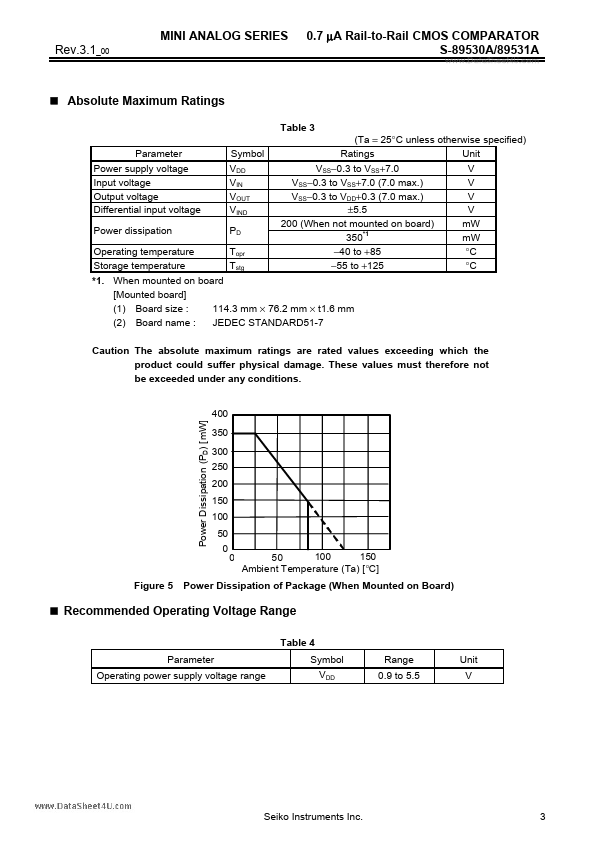
MINI ANALOG SERIES Rev.3.1_00 0.7 μA Rail-to-Rail CMOS PARATOR S-89530A/89531A .. When mounted on board [Mounted board] (1) Board size : 114.3 mm × 76.2 mm × t1.6 mm (2) Board name.