Full PDF Text Transcription for SML25SCM650N2B (Reference)
Note: Below is a high-fidelity text extraction (approx. 800 characters) for
SML25SCM650N2B. For precise diagrams, and layout, please refer to the original PDF.
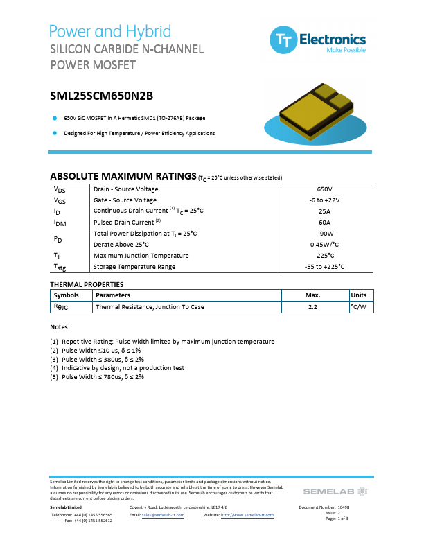
SILICON CARBIDE N-CHANNEL POWER MOSFET SML25SCM650N2B 650V SiC MOSFET In A Hermetic SMD1 (TO-276AB) Package Designed For High Temperature / Power Efficiency Applications ...
View more extracted text
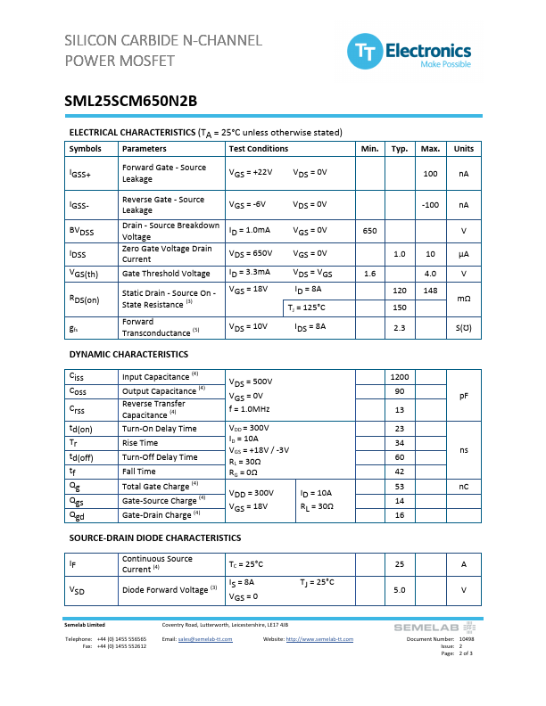
Package Designed For High Temperature / Power Efficiency Applications ABSOLUTE MAXIMUM RATINGS (TC = 25°C unless otherwise stated) VDS Drain - Source Voltage VGS Gate - Source Voltage ID Continuous Drain Current (1) Tc = 25°C IDM Pulsed Drain Current (2) PD Total Power Dissipation at TJ = 25°C Derate Above 25°C TJ Maximum Junction Temperature Tstg Storage Temperature Range THERMAL PROPERTIES Symbols Parameters RθJC Thermal Resistance, Junction To Case Notes (1) Repetitive Rating: Pulse width limited by maximum junction temperature (2) Pulse Width ≤10 us, δ ≤ 1% (3) Pulse Width ≤ 380us, δ ≤ 2% (4) Indicative by design, not
 SML25SCM650N2B Datasheet