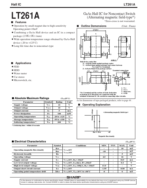
The following content is an automatically extracted verbatim text
from the original manufacturer datasheet and is provided for reference purposes only.
View original datasheet text
Hall IC
LT261A
2.9±0.2 1.9
2
0.4
3
0.4
0.95
X 4-R0.2 Hall device center line X : +0.05±0.23mm against package center Y : -0.05±0.1mm against package lead center between No.2 and No.3 terminals Z : 0.81±0.15mm from package surface Terminal connections 1.5±0.2 0.6 0.6 REG Hall + device H
0.3
1.1-0.1
0.16+0.10 -0.06
s Applications ¡FDD ¡HDD ¡Water meter ¡Car stereo ¡Microswitch, etc.
0.8
+0.2
-
(0to0.15)
s Absolute Maximum Ratings
Parameter Supply voltage Output voltage Output current Power dissipation Operating temperature Storage temperature Soldering temperature*1
*1 Soldering time : within 10 seconds
*No.3 terminal and the section of leads (both sides of package in X direction) are connected with the terminal of internal IC. Be careful in connecting other circuits.