Overview: VM149F Version Issue Date File Name
Total Page : A.002 : 2013-10-14 : SP-VM149F-A.002.doc
: 12 120mA, 10Bit Current Sinking VCM Driver with I2C Interface 新竹市科學園區展業一路 9 號 7 樓之 1
SILICON TOUCH TECHNOLOGY INC.
9-7F-1, Prosperity Road I, Science Based Industrial Park, Hsin-Chu, Taiwan 300, R.O.C.
Tel:886-3-5645656 Fax:886-3-5645626 VM149F
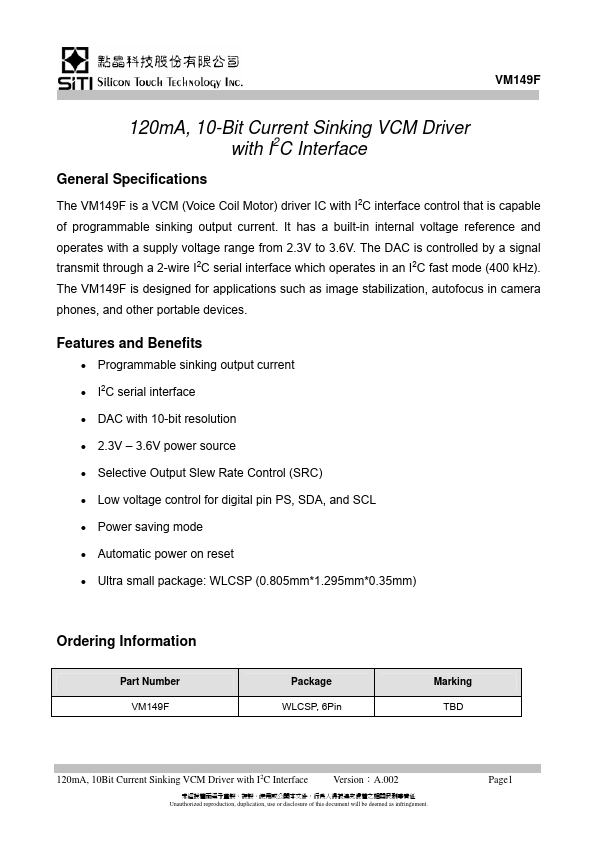
120mA, 10-Bit Current Sinking VCM Driver with I2C Interface
General Specifications
The VM149F is a VCM (Voice Coil Motor) driver IC with I2C interface control that is capable of programmable sinking output current. It has a built-in internal voltage reference and operates with a supply voltage range from 2.3V to 3.6V. The DAC is controlled by a signal transmit through a 2-wire I2C serial interface which operates in an I2C fast mode (400 kHz). The VM149F is designed for applications such as image stabilization, autofocus in camera phones, and other portable devices.