Download SI53307 Datasheet PDF
SI53307 page 2
Page 2
SI53307 page 3
Page 3

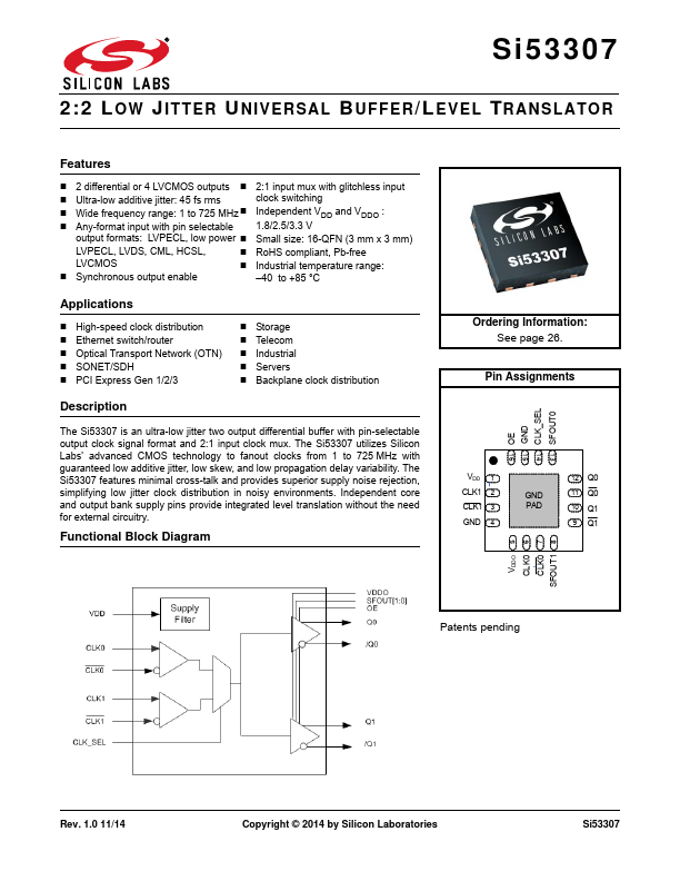
SI53307 Key Features

  • 2 differential or 4 LVCMOS outputs
  • 2:1 input mux with glitchless input
  • Ultra-low additive jitter: 45 fs rms
  • Wide frequency range: 1 to 725 MHz
  • Independent VDD and VDDO
  • Any-format input with pin selectable 1.8/2.5/3.3 V
  • Small size: 16-QFN (3 mm x 3 mm)
  • RoHS pliant, Pb-free
  • Synchronous output enable
  • Industrial temperature range: -40 to +85 °C

SI53307 Description

The Si53307 is an ultra-low jitter two output differential buffer with pin-selectable output clock signal format and 2:1 input clock mux. The Si53307 utilizes Silicon Labs' advanced CMOS technology to fanout clocks from 1 to 725 MHz with guaranteed low additive jitter, low skew, and low propagation delay variability.