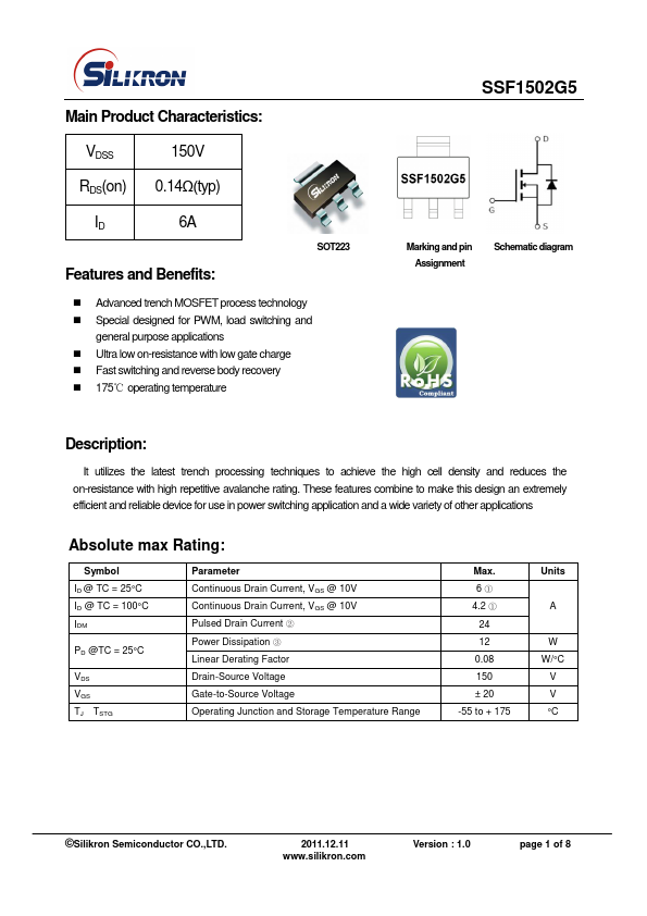
Main Product Characteristics:
VDSS
RDS(on)
150V
0.14Ω(typ)
ID 6A
SOT223
Features and Benefits:
Advanced trench MOSFET process technology
Special designed for PWM, load switching and
general purpose applications
Ultra low on-resistance with low gate charge
Fast switching and reverse body recovery
175℃ operating temperature
SSF1502G5
Marking and pin
Assignment
Schematic diagram
Description:
It utilizes the latest trench processing techniques to achieve the high cell density and reduces the
on-resistance with high repetitive avalanche rating. These features combine to make this design an extremely
efficient and reliable device for use in power switching application and a wide variety of other applications
Absolute max Rating:
Symbol
ID @ TC = 25°C
ID @ TC = 100°C
IDM
PD @TC = 25°C
VDS
VGS
TJ TSTG
Parameter
Continuous Drain Current, VGS @ 10V
Pulsed Drain Current ②
Power Dissipation ③
Linear Derating Factor
Drain-Source Voltage
Gate-to-Source Voltage
Operating Junction and Storage Temperature Range
Max.
6①
4.2 ①
24
12
0.08
150
±20
-55 to + 175
Units
A
W
W/°C
V
V
°C
©Silikron Semiconductor CO.,LTD.
2011.12.11
www.silikron.com
Version : 1.0
page 1 of 8