Datasheet Summary
19-OUTPUT PCIE GEN 3 BUFFER
Features
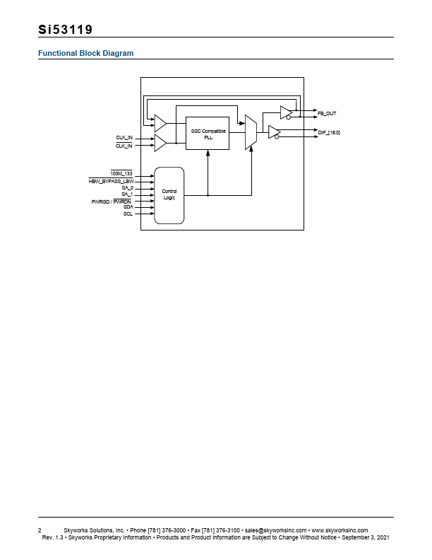
- Nineteen 0.7 V low-power, push-
- PLL or bypass mode pull HCSL PCIe Gen 3 outputs
- Spread spectrum tolerable
- 100 MHz /133 MHz PLL
- 1.05 to 3.3 V I/O supply voltage
- operation, supports PCIe and QPI
- PLL bandwidth SW SMBUS programming overrides the latch
- - value from HW pin
50 ps output-to-output skew
50 ps cyc-cyc jitter (PLL mode)
Low phase jitter (Intel QPI, PCIe Gen 1/2/3 mon clock pliant)
- -
9 selectable SMBUS addresses
SMBus address configurable to allow multiple buffers in a single
- -
Gen 3 SRNS pliant 100 ps input-to-output delay control network 3.3 V supply
- Extended Temperature: voltage...