Datasheet4U Logo Datasheet4U.com

CXM3513ER - High Power DP3T Switch

General Description

The CXM3513ER can be used in wireless communication systems, for example, triple-band W-CDMA handsets.

This IC has a decoder with 3 CMOS control inputs.

The Sony JPHEMT process is used for low insertion loss and low distortion characteristic.

Key Features

  • ‹ Low insertion loss: 0.36dB @900MHz, 0.43dB @1.95GHz ‹ 3 CMOS compatible control lines Package Small package size: 20-pin VQFN (2.4mm × 3.2mm × 0.9mm) Structure GaAs JPHEMT MMIC Absolute Maximum Ratings (Ta = 25°C).
  • Bias voltage.
  • Control voltage.
  • Operating temperature.
  • Storage temperature VDD Vctl Topr Tstg 7 5.
  • 35 to +85.
  • 65 to +150 V V °C °C This IC is ESD sensitive device. Special handling precautions are required. Sony reserves the right to change pro.

📥 Download Datasheet

Full PDF Text Transcription for CXM3513ER (Reference)

Note: Below is a high-fidelity text extraction (approx. 800 characters) for CXM3513ER. For precise diagrams, and layout, please refer to the original PDF.

High Power DP3T Switch with Logic Control 
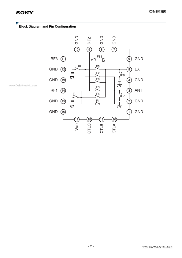
CXM3513ER Description The CXM3513ER can be used in wireless communication systems, for example, triple-band W-CDMA handsets. Thi...

View more extracted text
s communication systems, for example, triple-band W-CDMA handsets. This IC has a decoder with 3 CMOS control inputs. The Sony JPHEMT process is used for low insertion loss and low distortion characteristic. (Applications: Antenna switch for cellular handsets, triple-band W-CDMA) www.DataSheet4U.com Features ‹ Low insertion loss: 0.36dB @900MHz, 0.43dB @1.95GHz ‹ 3 CMOS compatible control lines Package Small package size: 20-pin VQFN (2.4mm × 3.2mm × 0.9mm) Structure GaAs JPHEMT MMIC Absolute Maximum Ratings (Ta = 25°C) Š Bias voltage Š Control voltage Š Operating temperature Š Storage temperature VDD Vctl Topr Tstg 7 5 –35