ICX098BQ
Description
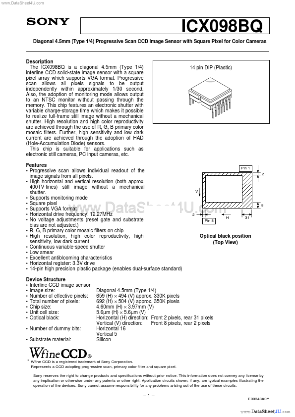
Vertical register transfer clock Vertical register transfer clock Vertical register transfer clock Vertical register transfer clock Protective transistor bias GND Signal output φSUB CSUB GND Pin No. 8 9 10 11 12 13 14 φRG VDD Symbol VDD GND φSUB CSUB φRG Hφ1 Hφ2 Hφ1 H φ2 Vφ 1 1 Note) 14 Description Supply voltage GND Substrate clock Substrate bias∗1 Reset gate clock Horizontal register transfer clock Horizontal register transfer clock ∗1 DC bias is generated within the CCD, so that this pin should be grounded externally through a capacitance of 0.1µF.
Key Features
- Progressive scan allows individual readout of the image signals from all pixels
- High horizontal and vertical resolution (both approx. 400TV-lines) still image without a mechanical shutter
- Supports monitoring mode
- Square pixel
- Supports VGA format
- Horizontal drive frequency: 12.27MHz
- No voltage adjustments (reset gate and substrate bias are not adjusted.)
- R, G, B primary color mosaic filters on chip
- High resolution, high color reproductivity, high sensitivity, low dark current
- Continuous variable-speed shutter