CW01DB1
Description
Specifications
Parameter VLL VDD VDX
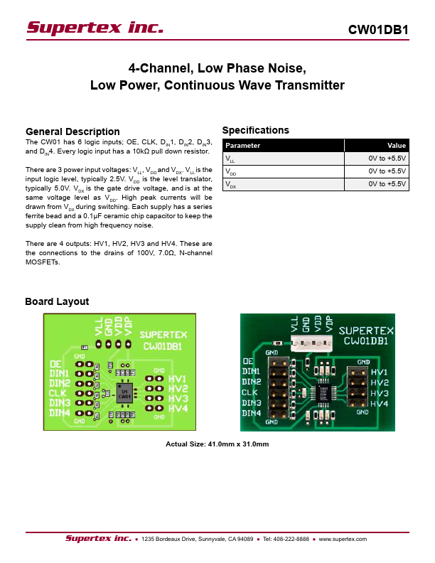
The CW01 has 6 logic inputs; OE, CLK, DIN1, DIN2, DIN3, and DIN4. Every logic input has a 10kΩ pull down resistor. There are 3 power input voltages: VLL, VDD and VDX. VLL is the input logic level, typically 2.5V. VDD is the level translator, typically 5.0V. VDX is the gate drive voltage, and is at the same voltage level as VDD. High peak currents will be drawn from VDX during switching. Each supply has a series ferrite bead and a 0.1µF ceramic chip capacitor to keep the supply clean from high frequency noise. There are 4 outputs: HV1, HV2, HV3 and HV4. These are the connections to the drains of 100V, 7.0Ω, N-channel MOSFETs.
Value 0V to +5.5V 0V to +5.5V 0V to +5.5V
Board Layout
Actual Size: 41.0mm x 31.0mm
Supertex inc.
- 1235 Bordeaux Drive, Sunnyvale, CA 94089
- Tel: 408-222-8888
- .supertex.
Datasheet pdf
- http://..net/
.Data Sheet.co.kr
CW01 Demoboard Circuit Diagram
GND VDD VDP FB2 C1 0.1µF C2 0.1µF VLL...