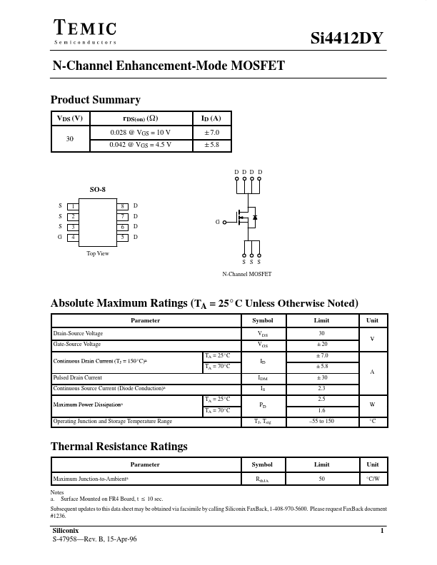
Si4412DY Description
Surface Mounted on FR4 Board, t v 10 sec. Subsequent updates to this data sheet may be obtained via facsimile by calling Siliconix FaxBack, 1-408-970-5600. Please request FaxBack document #1236.
Si4412DY is N-Channel Enhancement-Mode MOSFET manufactured by TEMIC Semiconductors.
| Manufacturer | Part Number | Description |
|---|---|---|
| Si4412ADY | N-Channel 30-V (D-S) MOSFET |
Surface Mounted on FR4 Board, t v 10 sec. Subsequent updates to this data sheet may be obtained via facsimile by calling Siliconix FaxBack, 1-408-970-5600. Please request FaxBack document #1236.