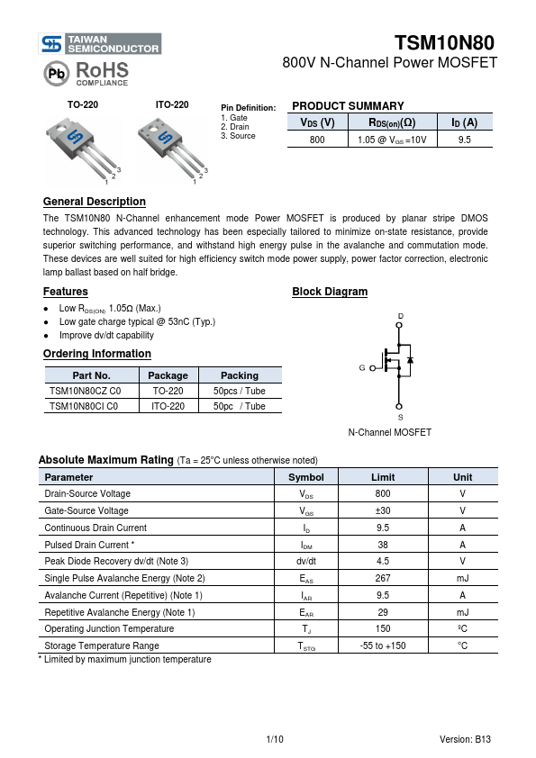
Datasheet4U Logo Datasheet4U.com

TSM10N80CI - 800V N-Channel Power MOSFET

This page provides the datasheet information for the TSM10N80CI, a member of the TSM10N80 800V N-Channel Power MOSFET family.

Description

The TSM10N80 N-Channel enhancement mode Power MOSFET is produced by planar stripe DMOS technology.

This advanced technology has been especially tailored to minimize on-state resistance, provide superior switching performance, and withstand high energy pulse in the avalanche and commutation mode.

Features

  • Low RDS(ON) 1.05Ω (Max. ) Low gate charge typical @ 53nC (Typ. ) Improve dv/dt capability Block Diagram Ordering Information Part No. TSM10N80CZ C0 TSM10N80CI C0 Package TO-220 ITO-220 Packing 50pcs / Tube 50pc / Tube N-Channel MOSFET Absolute Maximum Rating (Ta = 25oC unless otherwise noted) Parameter Drain-Source Voltage Gate-Source Voltage Continuous Drain Current Pulsed Drain Current.
  • Peak Diode Recovery dv/dt (Note 3) Single Pulse Avalanche Energy (Note 2) Avalanch.

📥 Download Datasheet

Datasheet preview – TSM10N80CI

Datasheet Details

Part number TSM10N80CI
Manufacturer Taiwan Semiconductor
File Size 497.95 KB
Description 800V N-Channel Power MOSFET
Datasheet download datasheet TSM10N80CI Datasheet
Additional preview pages of the TSM10N80CI datasheet.
Other Datasheets by Taiwan Semiconductor

Full PDF Text Transcription

Click to expand full text
TSM10N80 800V N-Channel Power MOSFET TO-220 ITO-220 Pin Definition: 1. Gate 2. Drain 3. Source PRODUCT SUMMARY VDS (V) RDS(on)(Ω) 800 1.05 @ VGS =10V ID (A) 9.5 General Description The TSM10N80 N-Channel enhancement mode Power MOSFET is produced by planar stripe DMOS technology. This advanced technology has been especially tailored to minimize on-state resistance, provide superior switching performance, and withstand high energy pulse in the avalanche and commutation mode. These devices are well suited for high efficiency switch mode power supply, power factor correction, electronic lamp ballast based on half bridge. Features ● ● ● Low RDS(ON) 1.05Ω (Max.) Low gate charge typical @ 53nC (Typ.) Improve dv/dt capability Block Diagram Ordering Information Part No.
Published: |