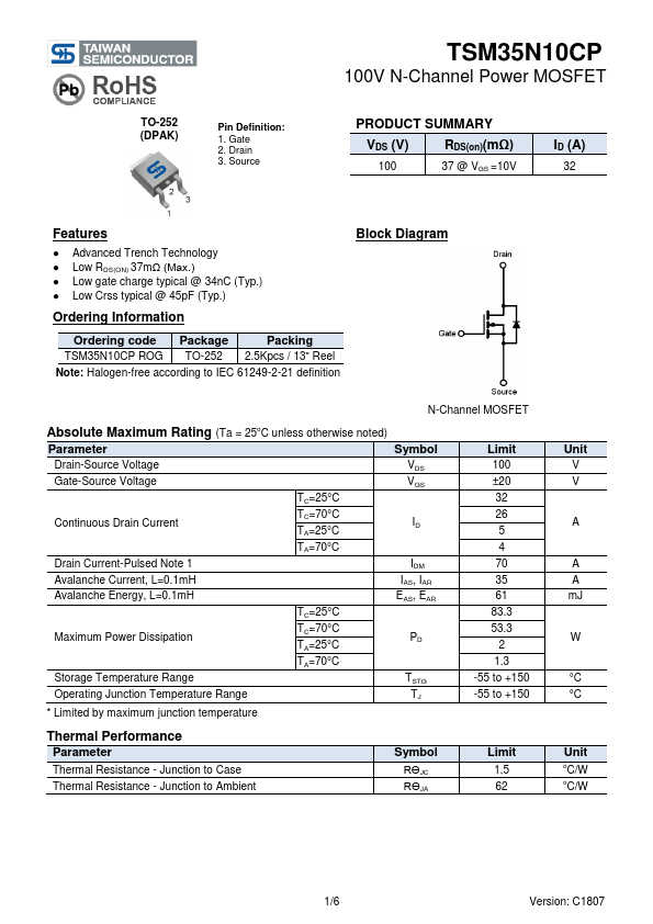
Datasheet4U Logo Datasheet4U.com

TSM35N10CP - 100V N-Channel Power MOSFET

This page provides the datasheet information for the TSM35N10CP, a member of the TSM35N10 100V N-Channel Power MOSFET family.

Description

only.

No license, express or implied, to any intellectual property rights is granted by this document.

Features

  • Advanced Trench Technology Low RDS(ON) 37mΩ (Max. ) Low gate charge typical @ 34nC (Typ. ) Low Crss typical @ 45pF (Typ. ) Block Diagram Ordering Information Part No. TSM35N10CP ROG Package TO-252 Packing 2.5Kpcs / 13” Reel Note: “G” denote for Halogen Free Product N-Channel MOSFET Absolute Maximum Rating (Ta = 25oC unless otherwise noted) Parameter Drain-Source Voltage Gate-Source Voltage TC=25° C TC=70° C TA=25° C TA=70° C Symbol VDS VGS Limit 100 ±20 32 26 5 4 70.

📥 Download Datasheet

Datasheet preview – TSM35N10CP

Datasheet Details

Part number TSM35N10CP
Manufacturer Taiwan Semiconductor
File Size 572.70 KB
Description 100V N-Channel Power MOSFET
Datasheet download datasheet TSM35N10CP Datasheet
Additional preview pages of the TSM35N10CP datasheet.
Other Datasheets by Taiwan Semiconductor

Full PDF Text Transcription

Click to expand full text
TSM35N10 100V N-Channel Power MOSFET TO-252 (DPAK) Pin Definition: 1. Gate 2. Drain 3. Source PRODUCT SUMMARY VDS (V) 100 RDS(on)(mΩ) 37 @ VGS =10V ID (A) 32 Features ● ● ● ● Advanced Trench Technology Low RDS(ON) 37mΩ (Max.) Low gate charge typical @ 34nC (Typ.) Low Crss typical @ 45pF (Typ.) Block Diagram Ordering Information Part No. TSM35N10CP ROG Package TO-252 Packing 2.5Kpcs / 13” Reel Note: “G” denote for Halogen Free Product N-Channel MOSFET Absolute Maximum Rating (Ta = 25oC unless otherwise noted) Parameter Drain-Source Voltage Gate-Source Voltage TC=25° C TC=70° C TA=25° C TA=70° C Symbol VDS VGS Limit 100 ±20 32 26 5 4 70 35 61 83.3 53.3 2 1.3 -55 to +150 -55 to +150 Unit V V Continuous Drain Current ID A Drain Current-Pulsed Note 1 Avalanche Current, L=0.
Published: |