Click to expand full text
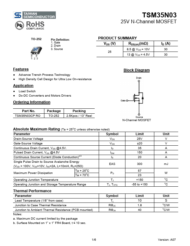
TSM35N03
25V N-Channel MOSFET
TO-252
Pin Definition: 1. Gate 2. Drain 3. Source
PRODUCT SUMMARY
VDS (V)
RDS(on)(mΩ)
25 8.5 @ VGS = 10V 13 @ VGS = 4.5V
ID (A)
30 30
Features
● Advance Trench Process Technology ● High Density Cell Design for Ultra Low On-resistance
Application
● Load Switch ● Dc-DC Converters and Motors Drivers
Ordering Information
Block Diagram
Part No. TSM35N03CP RO
Package TO-252
Packing 2.5Kpcs / 13” Reel
N-Channel MOSFET
Absolute Maximum Rating (Ta = 25oC unless otherwise noted)
Parameter
Symbol
Drain-Source Voltage
VDS
Gate-Source Voltage Continuous Drain Current, VGS @4.5V.
VGS ID
Pulsed Drain Current, VGS @4.