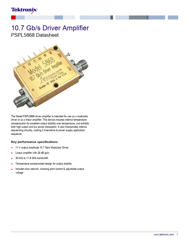
PSPL5868 Description
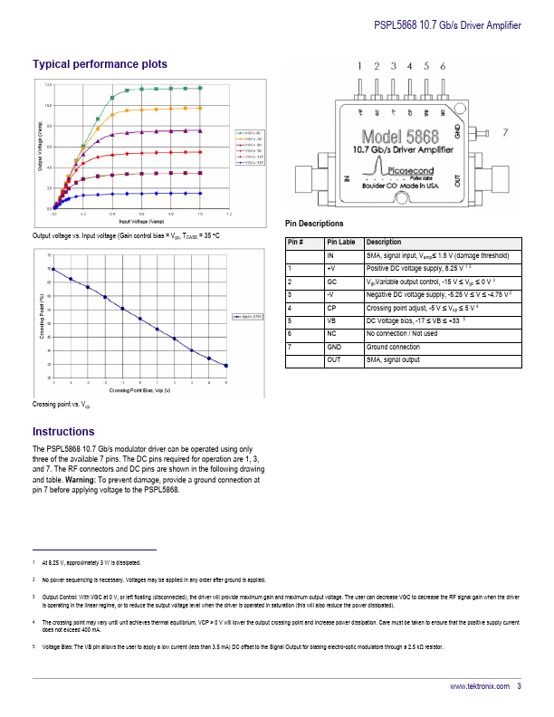
Vcp Instructions The PSPL5868 10.7 Gb/s modulator driver can be operated using only three of the available 7 pins. The DC pins required for operation are 1, 3, and 7. The RF connectors and DC pins are shown in the following drawing and table.