7UL1T02FU
7UL1T02FU is 2-Input NOR Gate manufactured by Toshiba.
Description
- 2-Input NOR Gate with Level Shifting
2. Features
(1) Wide operating voltage range: VCC = 2.3 to 3.6 V (2) Output level up to supply VCC CMOS level: 1.65 V to 3.6 V (VCC = 3.6 V) (3) Output level down to supply VCC CMOS level: 3.6 V to 2.3 V (VCC = 2.3 V) (4) 3.6 V tolerant inputs (5) 3.6 V power down protection output
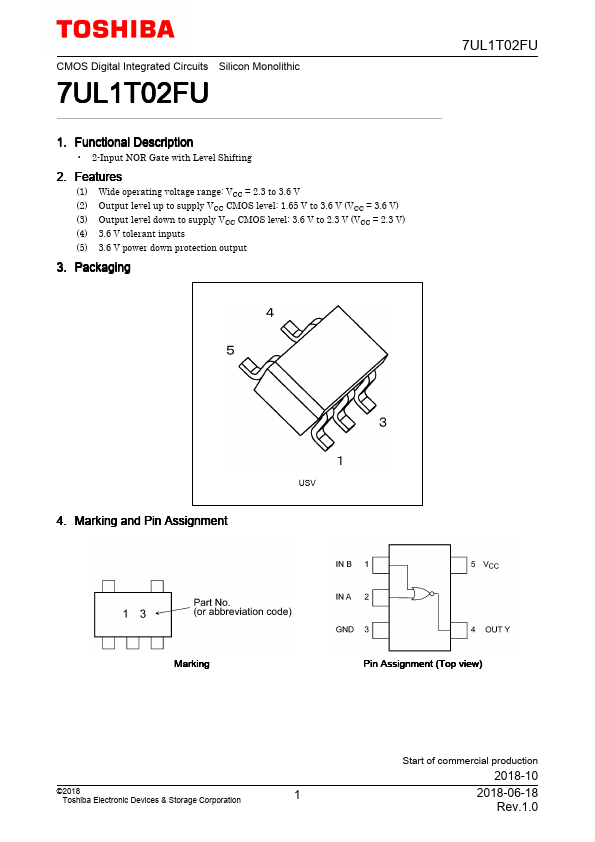
3. Packaging
4. Marking and Pin Assignment
Marking
Pin Assignment (Top view)
©2018 Toshiba Electronic Devices & Storage Corporation
Start of mercial production
2018-10
2018-06-18 Rev.1.0
5. IEC Logic Symbol
6. Truth Table
L LH LHL HL L HH L
7. Absolute Maximum Ratings (Note) (Unless otherwise specified, Ta = 25 )
Characteristics
Symbol
Note
Rating
Unit
Supply voltage
-0.5 to 4.6
Input voltage
-0.5 to 4.6
DC output voltage
VOUT
(Note 1)
-0.5 to 4.6
(Note 2)
-0.5 to VCC + 0.5
Input diode current...