TB7109F
TB7109F is Power supply IC manufactured by Toshiba.
TOSHIBA BiCD Integrated Circuit Silicon Monolithic
Power supply IC for LNB
The TB7109F is single chip power supply ICs for LNB that integrated buck DC-DC converter section utilizing a chopper circuit and series regulator section. The TB7109F contains high-speed P-channel MOSFETs for the high side main switch to achieve high efficiency. And series regulator section is fed into a overcurrent circuit of fold buck type, and it protects this product from the short circuit state of the load.
Features
- Output current: DC-DC Converter section IOUT1 = 500mA(max.) Series Regulator section IOUT2 = 400mA(max.)
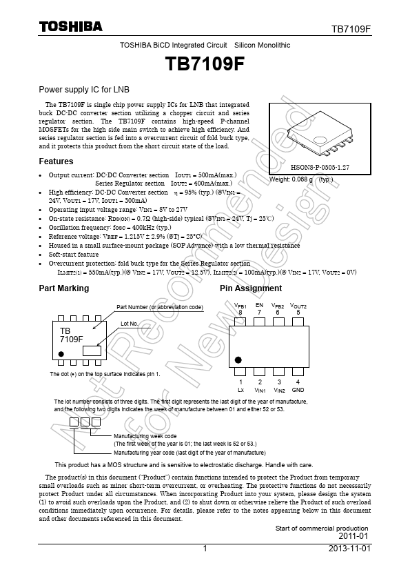
HSON8-P-0505-1.27 Weight: 0.068 g (typ.)
- High efficiency: DC-DC...