Datasheet4U Logo Datasheet4U.com

TC4011BF - Quad 2 Input NAND Gate

This page provides the datasheet information for the TC4011BF, a member of the TC4011BP Quad 2 Input NAND Gate family.

📥 Download Datasheet

Datasheet preview – TC4011BF

Datasheet Details

Part number TC4011BF
Manufacturer Toshiba
File Size 206.67 KB
Description Quad 2 Input NAND Gate
Datasheet download datasheet TC4011BF Datasheet
Additional preview pages of the TC4011BF datasheet.
Other Datasheets by Toshiba

Full PDF Text Transcription

Click to expand full text
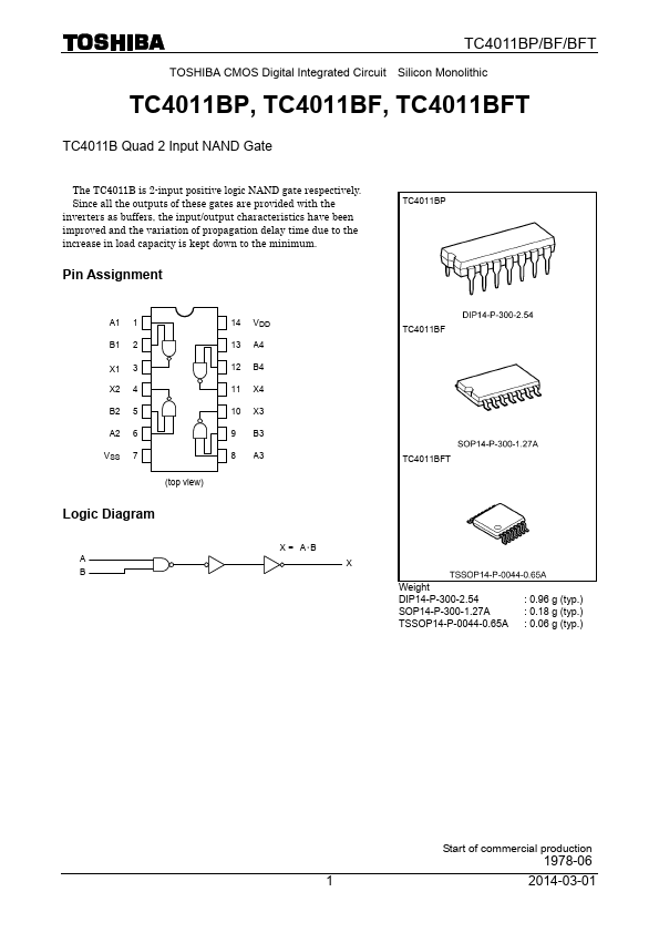
TC4011BP/BF/BFT TOSHIBA CMOS Digital Integrated Circuit Silicon Monolithic TC4011BP, TC4011BF, TC4011BFT TC4011B Quad 2 Input NAND Gate The TC4011B is 2-input positive logic NAND gate respectively. Since all the outputs of these gates are provided with the inverters as buffers, the input/output characteristics have been improved and the variation of propagation delay time due to the increase in load capacity is kept down to the minimum. Pin Assignment TC4011BP A1 1 B1 2 X1 3 X2 4 B2 5 A2 6 VSS 7 (top view) Logic Diagram A B 14 VDD 13 A4 12 B4 11 X4 10 X3 9 B3 8 A3 X = A・B X TC4011BF TC4011BFT Weight DIP14-P-300-2.54 SOP14-P-300-1.27A TSSOP14-P-0044-0.65A : 0.96 g (typ.) : 0.18 g (typ.) : 0.06 g (typ.
Published: |