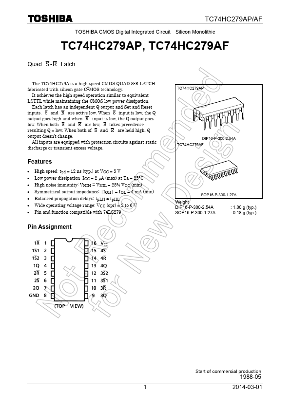
Datasheet4U Logo Datasheet4U.com

TC74HC279AP - Quad S-R Latch

Download the TC74HC279AP datasheet PDF. This datasheet also covers the TC74HC279 variant, as both devices belong to the same quad s-r latch family and are provided as variant models within a single manufacturer datasheet.

Key Features

  • High speed: tpd = 12 ns (typ. ) at VCC = 5 V.
  • Low power dissipation: ICC = 2 μA (max) at Ta = 25°C.
  • High noise immunity: VNIH = VNIL = 28% VCC (min).
  • Symmetrical output impedance: |IOH| = IOL = 4 mA (min).
  • Balanced propagation delays: tpLH ∼.
  • tpHL.
  • Wide operating voltage range: VCC (opr) = 2 to 6 V.
  • Pin and function compatible with 74LS279 Pin Assignment TC74HC279AP TC74HC279AF Weight DIP16-P-300-2.54A SOP16-P-300-1.27A :.

📥 Download Datasheet

Note: The manufacturer provides a single datasheet file (TC74HC279_Toshiba.pdf) that lists specifications for multiple related part numbers.

Full PDF Text Transcription for TC74HC279AP (Reference)

Note: Below is a high-fidelity text extraction (approx. 800 characters) for TC74HC279AP. For precise diagrams, and layout, please refer to the original PDF.

TC74HC279AP/AF TOSHIBA CMOS Digital Integrated Circuit Silicon Monolithic TC74HC279AP, TC74HC279AF Quad S -R Latch The TC74HC279A is a high speed CMOS QUAD S-R LATCH fabr...

View more extracted text
uad S -R Latch The TC74HC279A is a high speed CMOS QUAD S-R LATCH fabricated with silicon gate C2MOS technology. It achieves the high speed operation similar to equivalent LSTTL while maintaining the CMOS low power dissipation. Each latch has an independent Q output and Set and Reset inputs. S and R are active low. When S input is low, the Q output goes high and when R input is low, the Q output goes low. When both S and R are low, S takes precedence resulting Q = low. When both of S and R are held high, Q output doesn’t change. All inputs are equipped with protection circuits against static discharge or transient excess v