Datasheet Details
| Part number | TC74HC4050AFT |
|---|---|
| Manufacturer | Toshiba |
| File Size | 218.44 KB |
| Description | HEX BUFFER/CONVERTER |
| Datasheet | TC74HC4050AFT TC74HC4049AFT Datasheet (PDF) |
|
|
Overview: TC74HC4049AFT,TC74HC4050AFT CMOS Digital Integrated Circuits Silicon Monolithic TC74HC4049AFT,TC74HC4050AFT 1.
This datasheet includes multiple variants, all published together in a single manufacturer document.
| Part number | TC74HC4050AFT |
|---|---|
| Manufacturer | Toshiba |
| File Size | 218.44 KB |
| Description | HEX BUFFER/CONVERTER |
| Datasheet | TC74HC4050AFT TC74HC4049AFT Datasheet (PDF) |
|
|
|
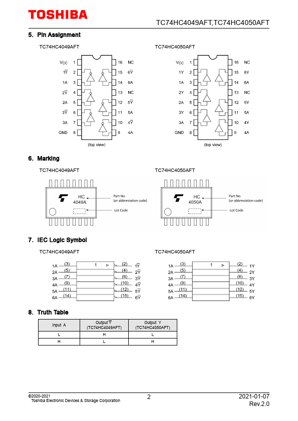
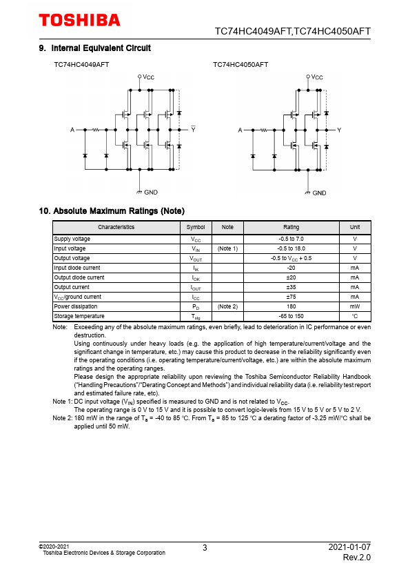
• Hex Buffer TC74HC4049AFT: HEX BUFFER/CONVERTER (INVERTING) TC74HC4050AFT: HEX BUFFER/CONVERTER 2.
General The TC74HC4049AFT and TC74HC4050AFT are high speed CMOS HEX BUFFERs fabricated with silicon gate C2MOS technology.
They achieve the high speed operation similar to equivalent LSTTL while maintaining the CMOS low power dissipation.
| Part Number | Description |
|---|---|
| TC74HC4050AF | HEX BUFFER/CONVERTER |
| TC74HC4050AP | HEX BUFFER/CONVERTER |
| TC74HC4002AF | Dual 4-Input NOR Gate |
| TC74HC4002AP | Dual 4-Input NOR Gate |
| TC74HC40102AF | Dual BCD Programmable Down Counter |
| TC74HC40102AP | Dual BCD Programmable Down Counter |
| TC74HC40103AF | 8-Bit Binary Programmable Down Counter |
| TC74HC40103AP | 8-Bit Binary Programmable Down Counter |
| TC74HC40105AF | 4-Bit x 16 Word FIFO Register |
| TC74HC40105AP | 4-Bit x 16 Word FIFO Register |