TC74HC4049AP,TC74HC4050AP
CMOS Digital Integrated Circuits Silicon Monolithic
TC74HC4049AP,TC74HC4050AP
1. Functional Description
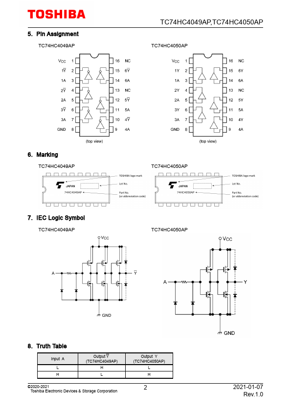
• Hex Buffer
TC74HC4049AP: HEX BUFFER/CONVERTER (INVERTING)
TC74HC4050AP: HEX BUFFER/CONVERTER
2. General
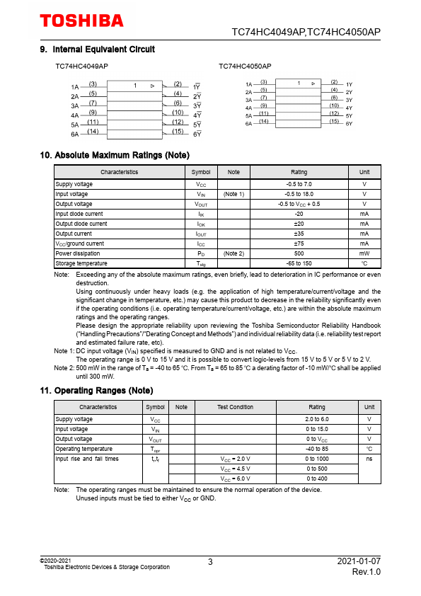
The TC74HC4049AP and TC74HC4050AP are high speed CMOS HEX BUFFERs fabricated with silicon gate
C2MOS technology.
They achieve the high speed operation similar to equivalent LSTTL while maintaining the CMOS low power
dissipation.
The TC74HC4049AP is an inverting buffer, while the TC74HC4050AP is a non-inverting buffer. The internal
circuits are composed of 3-stages (TC74HC4049AP) or 2-stages (TC74HC4050AP) of inverter, which provided
high noise immunity and stable output.
Input protection circuits are different from those of other high speed CMOS IC's. They eliminate the diodes on
the VCC side thus providing of logic-level conversion from high-level voltages up to 15 V to low-level voltages.
They are useful for battery back up circuits, because input voltage can be applied on IC's which are not biased
by VCC.
3. Features
(1) High speed: tpd = 9 ns (typ.) at VCC = 5.0 V
(2) Low power dissipation: ICC = 1.0 µA (max) at Ta = 25 �
(3) High noise immunity: VNIH = VNIL = 28 % VCC (min)
(4) Symmetrical Output impedance: |IOH| = IOL = 6 mA (min)
(5) Balanced propagation delays: tPLH ≈ tPHL
(6) Wide operating voltage range: VCC(opr) = 2.0 V to 6.0 V
(7) Power-down protection is provided on all inputs.
4. Packaging
DIP16
©2020-2021
1
Toshiba Electronic Devices & Storage Corporation
Start of commercial production
1986-05
2021-01-07
Rev.1.0