Key Specifications
Operating Voltage: 3 V
Max Voltage (typical range): 7 V
Length: 1.6 mm
Width: 1.2 mm
Max Operating Temp: 85 °C
Min Operating Temp: -40 °C
| Part | TC75S56FE |
|---|---|
| Description | Single Comparator |
| Category | Comparator |
| Manufacturer | Toshiba |
| Size | 347.22 KB |
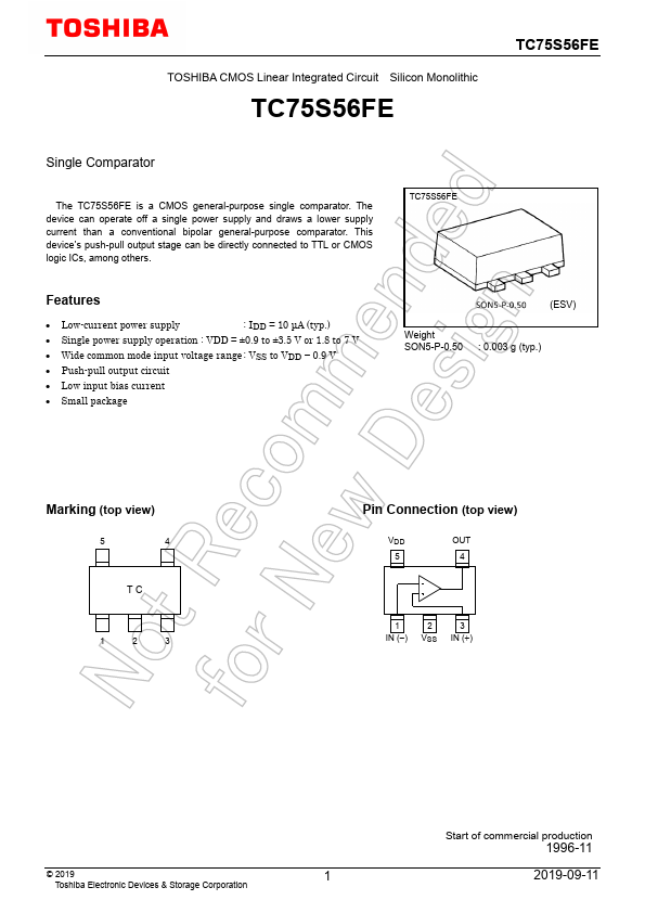
Single Comparator
Low-current power supply : IDD = 10 μA (typ.)
Single power supply operation : VDD = ±0.9 to ±3.5 V or 1.8 to 7 V
Wide common mode input voltage range : VSS to VDD
Push-pull output circuit
Low input bias current
Pricing from 0.1617 USD, available from Win Source and Worldway Electronics.
Powered by Octopart
Price & Availability
| Seller | Price Breaks | Buy |
|---|---|---|
| Win Source | 360+ : 0.1617 USD 870+ : 0.1328 USD 1340+ : 0.1294 USD 1855+ : 0.1247 USD |
View Offer |
| Worldway Electronics | 7+ : 0.0258 USD 10+ : 0.0252 USD 100+ : 0.0245 USD 500+ : 0.0237 USD |
View Offer |