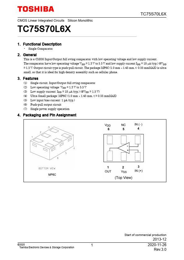
TC75S70L6X Overview
Key Specifications
Mount Type: Surface Mount
Pins: 6
Max Operating Temp: 85 °C
Min Operating Temp: -40 °C
Key Features
- Single Comparator
| Part | TC75S70L6X |
|---|---|
| Description | Single Comparator |
| Category | Comparator |
| Manufacturer | Toshiba |
| Size | 240.81 KB |
Mount Type: Surface Mount
Pins: 6
Max Operating Temp: 85 °C
Min Operating Temp: -40 °C
| Seller | Inventory | Price Breaks | Buy |
|---|---|---|---|
| DigiKey | 4820 | 1+ : 0.41 USD 10+ : 0.283 USD 25+ : 0.2516 USD 100+ : 0.2178 USD |
View Offer |
| DigiKey | 4820 | 1+ : 0.41 USD 10+ : 0.283 USD 25+ : 0.2516 USD 100+ : 0.2178 USD |
View Offer |
| Part Number | Manufacturer | Description |
|---|---|---|
| LM339A | NXP Semiconductors | Quad voltage comparator |
| CMP04 | Analog Devices | Quad Low Power/ Precision Comparator |
| CMP05 | Analog Devices | High Speed Precision Comparator |