TC75W56L8X
Key Features
- Single power supply operation z mon mode input voltage range: VSS to VDD
- Push-pull output circuit
- Low input bias current
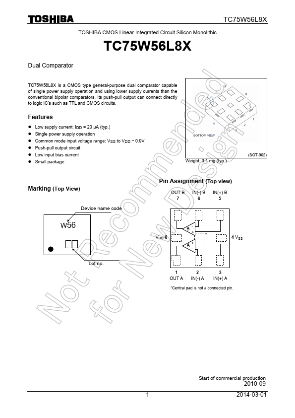
- 4 VSS 1 2 OUT A IN(-) A 3 IN(+) A *Central pad is not a connected pin. Start of mercial production 2010-09 1 2014-03-01