TC75W70L8X Overview
Key Features
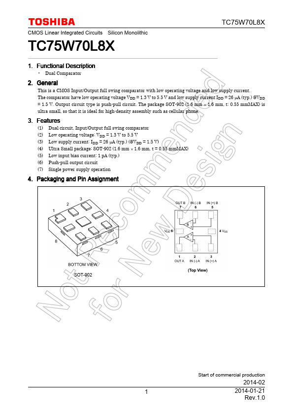
- Dual Comparator
| Part | TC75W70L8X |
|---|---|
| Description | Dual Comparator |
| Category | Comparator |
| Manufacturer | Toshiba |
| Size | 251.86 KB |
| Part Number | Manufacturer | Description |
|---|---|---|
| LM339A | NXP Semiconductors | Quad voltage comparator |
| CMP04 | Analog Devices | Quad Low Power/ Precision Comparator |
| CMP05 | Analog Devices | High Speed Precision Comparator |