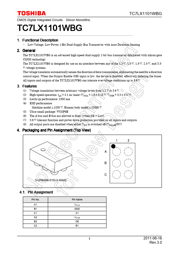
• Part: TC7LX1101WBG
  • Description: 1-Bit Dual-Supply Bus Transceiver
  • Manufacturer: Toshiba
  • Size: 226.50 KB
Download TC7LX1101WBG Datasheet PDF
TC7LX1101WBG page 2
Page 2
TC7LX1101WBG page 3
Page 3

TC7LX1101WBG Datasheet Text

CMOS Digital Integrated Circuits Silicon Monolithic TC7LX1101WBG TC7LX1101WBG 1. Functional Description - Low-Voltage, Low-Power 1-Bit Dual-Supply Bus Transceiver with Auto Direction Sensing 2. General The TC7LX1101WBG is an advanced high-speed dual-supply 1-bit bus transceiver fabricated with silicon-gate CMOS technology. The TC7LX1101WBG is designed for use as an interface between any of the 1.2-V, 1.5-V, 1.8-V, 2.5-V, and 3.3V voltage systems. The voltage translator automatically senses the direction of data transmission, eliminating the need for a direction control input. When the Output Enable (OE) input is low, the device is disabled, effectively isolating the buses. All inputs and outputs of the TC7LX1101WBG can tolerate overvoltage conditions up to 3.6 V. 3. Features (1) Voltage translation between arbitrary voltage levels from 1.2 V to 3.6 V. (2) High-speed operation: tpd = 5.1 ns (max) (VCCA = 1.8 ± 0.15 V, VCCB = 3.3 ± 0.3 V) (3) Latch-up performance: ±300 mA (4) ESD performance: Machine model ≥ ±200 V, Human body model ≥ ±2000 V (5) Ultra-small package: WCSP6B (6) The A-bus and B-bus are allowed to float. (when OE = Low) (7) 3.6-V tolerant function and power-down protection provided on all inputs and outputs. (8) All output ports are disabled when either VCC is switched off (VCCA/B=0V) 4. Packaging and Pin Assignment (Top View) S-UFBGA6-0102-0.40A02 4.1. Pin Assignment Pin No. A1 B1 C1 A2 B2 C2 Pin Name VCCA GND A1 VCCB OE B1 1 2011-06-16 Rev.3.0 5. Marking TC7LX1101WBG 6. Block Diagram Fig. 5.1 Marking Fig. 6.1 Block Diagram 2 2011-06-16 Rev.3.0 TC7LX1101WBG 7. Internal Equivalent Circuit The TC7LX1101WBG does not have a control signal that controls the direction of data flow between A and B. In a DC state, the output circuit holds either...