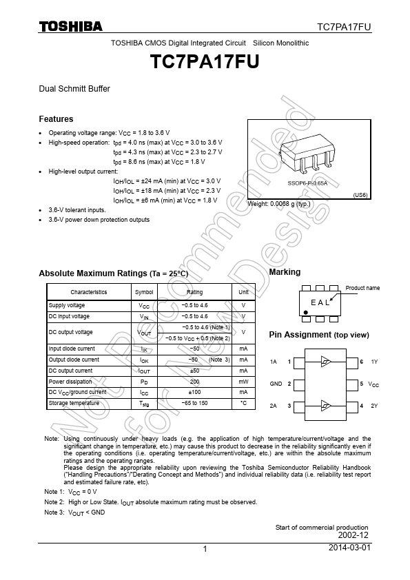
TC7PA17FU
TOSHIBA CMOS Digital Integrated Circuit Silicon Monolithic
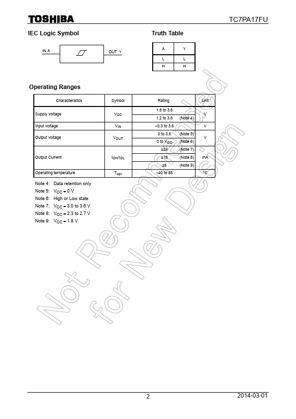
TC7PA17FU
Dual Schmitt Buffer
Features
• Operating voltage range: VCC = 1.8 to 3.6 V
• High-speed operation: tpd = 4.0 ns (max) at VCC = 3.0 to 3.6 V
tpd = 4.3 ns (max) at VCC = 2.3 to 2.7 V
tpd = 8.6 ns (max) at VCC = 1.8 V
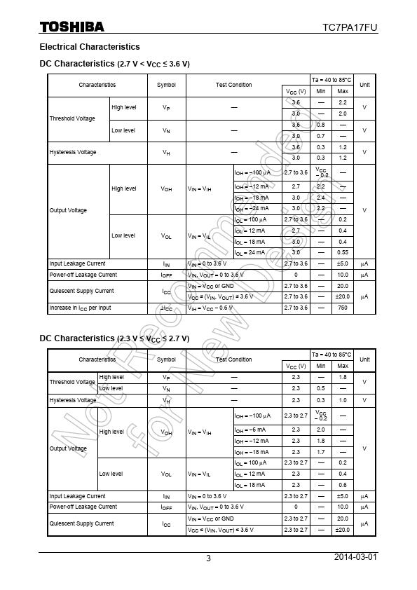
• High-level output current:
IOH/IOL = ±24 mA (min) at VCC = 3.0 V
IOH/IOL = ±18 mA (min) at VCC = 2.3 V
IOH/IOL = ±6 mA (min) at VCC = 1.8 V
• 3.6-V tolerant inputs.
• 3.6-V power down protection outputs
Weight: 0.0068 g (typ.)
(US6)
Absolute Maximum Ratings (Ta = 25°C)
Characteristics
Supply voltage
DC input voltage
DC output voltage
Input diode current
Output diode current
DC output current
Power dissipation
DC VCC/ground current
Storage temperature
Symbol
VCC
VIN
VOUT
IIK
IOK
IOUT
PD
ICC
Tstg
Rating
Unit
−0.5 to 4.6
V
−0.5 to 4.6
V
−0.5 to 4.6 (Note 1)
V
−0.5 to VCC + 0.5 (Note 2)
−50
mA
−50 (Note 3) mA
±50
mA
200
mW
±100
mA
−65 to 150
°C
Marking
EAL
Product name
Pin Assignment (top view)
1A 1
GND 2
2A 3
6 1Y
5 VCC
4 2Y
Note: Using continuously under heavy loads (e.g. the application of high temperature/current/voltage and the
significant change in temperature, etc.) may cause this product to decrease in the reliability significantly even if
the operating conditions (i.e. operating temperature/current/voltage, etc.) are within the absolute maximum
ratings and the operating ranges.
Please design the appropriate reliability upon reviewing the Toshiba Semiconductor Reliability Handbook
(“Handling Precautions”/“Derating Concept and Methods”) and individual reliability data (i.e. reliability test report
and estimated failure rate, etc).
Note 1: VCC = 0 V
Note 2: High or Low State. IOUT absolute maximum rating must be observed.
Note 3: VOUT < GND
Start of commercial production
2002-12
1
2014-03-01