TC7PB54FK Key Features
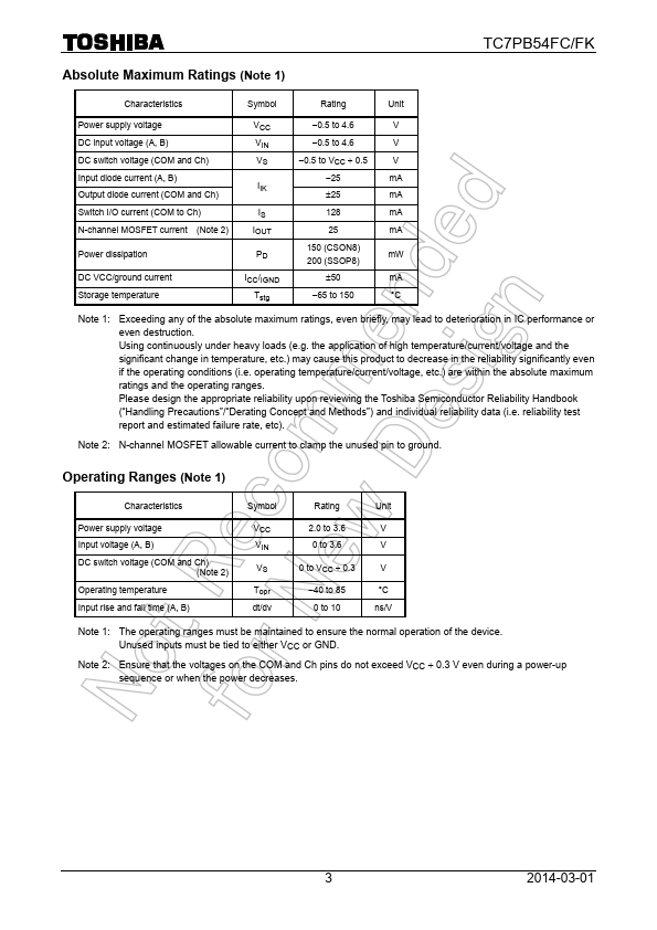
- Operating voltage range: VCC = 2 to 3.6 V
- High-speed operation: tpd = 70 ns (max) @ 2.7 V
- Very low ON-resistance: RON = 3 Ω (max) @ 2.7 V
- High latch-up immunity: Higher than or equal to ±300 mA
- ESD performance: Machine model ≥ ±200 V
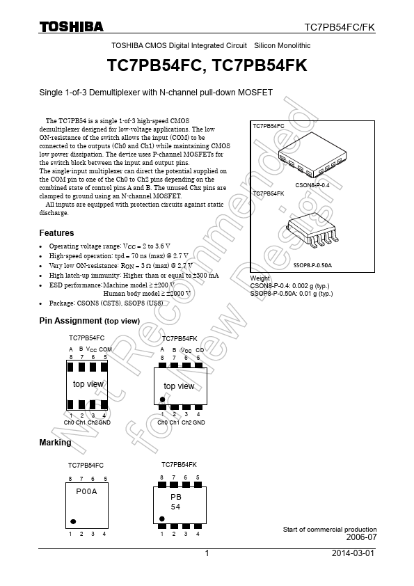
- Package: CSON8 (CST8), SSOP8 (US8)