TC7SB67CFU
TC7SB67CFU is Low-Capacitance Single Bus Switch manufactured by Toshiba.
- Part of the TC7SB66CFU comparator family.
- Part of the TC7SB66CFU comparator family.
TC7SB66CFU,TC7SB67CFU
CMOS Digital Integrated Circuits Silicon Monolithic
TC7SB66CFU,TC7SB67CFU
1. Functional Description
- Low-Capacitance Single Bus Switch (analog)
2. General
The TC7SB66CFU and TC7SB67CFU are low ON-resistance, high-speed CMOS 1-bit bus switches. These bus switches allow connections or disconnections to be made with minimal propagation delay while maintaining Low power dissipation which is the feature of CMOS. TC7SB66CFU requires the output enable (OE) input to be set low to place the output into the high impedance state,whereas the TC7SB67CFU requires the output enable (OE) input to be set high to place the output into the high impedance. These Bus switches consist of P-MOS and N-MOS structure, meaning these devices are suitable for analog signal transmission. All inputs are equipped with protector circuits to protect the device from static discharge.
3. Features
(1) AEC-Q100 (rev.H) Grade 1 qualified (Note 1) (2) Wide operating temperature range: Topr = -40 to 125
- (Note 2) (3) Operating voltage: VCC = 1.65 to 5.5 V (4) ON capacitance: CI/O = 10 p F Switch On (typ.) @VCC = 5.0 V (5) ON resistance: RON = 4 Ω (typ.) @VCC = 4.5 V, VIS = 0 V (6) Package: USV
Note 1: This device is pliant with the reliability requirements of AEC-Q100. For details, contact your Toshiba sales representative.
Note 2: For devices with the ordering part number ending in (CT. Topr = -40 to 85
- for the other devices.
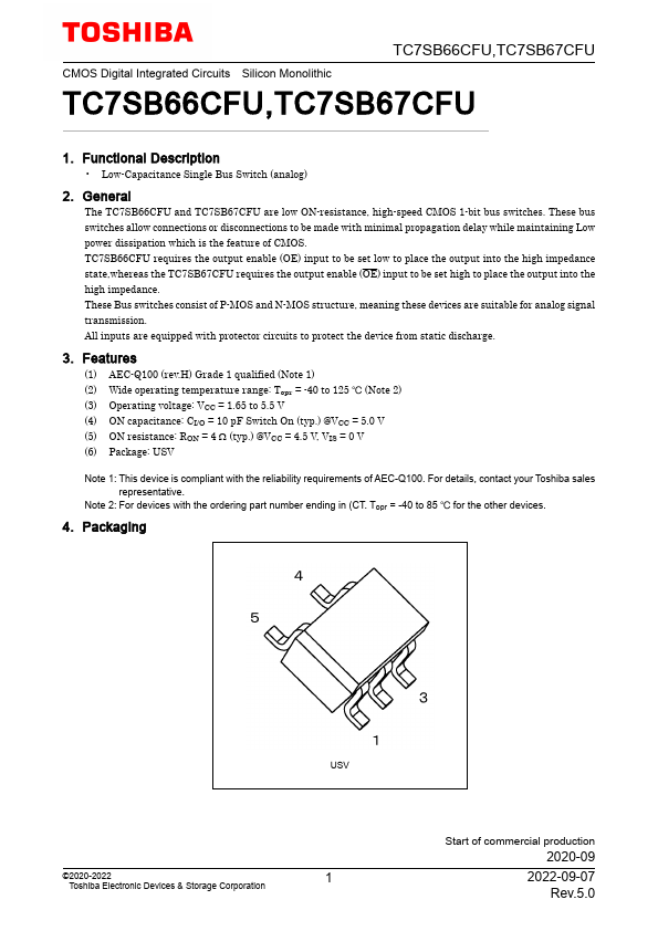
4. Packaging
©2020-2022
Toshiba Electronic Devices & Storage Corporation
Start of mercial production
2020-09
2022-09-07 Rev.5.0
5. Pin Assignment
TC7SB66CFU
TC7SB66CFU,TC7SB67CFU
6. Block Diagram
TC7SB66CFU
7. Principle of Operation 7.1. Truth Table
Input OE (TC7SB66CFU)
Input OE (TC7SB67CFU)
Function
A port = B port Disconnect
©2020-2022...