TC7SGU04FU
Features
- High output current
: ±8 m A (min) at VCC = 3 V
- Super high speed operation : tpd = 1.9 ns (typ.) at VCC = 3.3 V, 15p F
- Operating voltage range : VCC = 0.9 to 3.6 V
- 3.6-V tolerant input
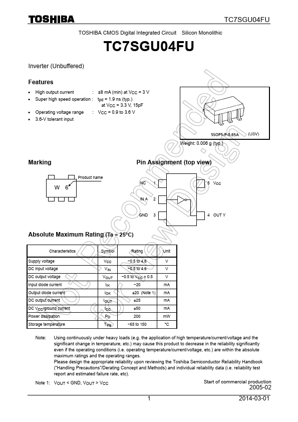
Weight: 0.006 g (typ.)
Marking
W6
Product name
Pin Assignment (top view)
NC 1 IN A 2 GND 3
5 VCC 4 OUT Y
Absolute Maximum Rating (Ta = 25°C)
Characteristics
Supply voltage DC input voltage DC output voltage Input diode current Output diode current DC output current DC VCC/ground current Power dissipation Storage temperature
Symbol
Rating
Unit
VCC VIN VOUT IIK IOK IOUT ICC PD Tstg
- 0.5 to 4.6
- 0.5 to 4.6
- 0.5 to VCC + 0.5
- 20 m A
±20 (Note 1) m A
±25 m A
±50 m A
200 m W
- 65 to 150
°C
Note:
Using continuously under heavy loads (e.g. the application of high temperature/current/voltage and the significant change in temperature, etc.) may cause this product to decrease in the reliability significantly even if the operating conditions (i.e. operating...