TC7SH07FE
TOSHIBA CMOS Digital Integrated Circuit Silicon Monolithic
TC7SH07FE
NON-Inverter (Open Drain)
Features
• High speed: tpZL = 3.7 ns (typ.) at VCC = 5 V, 15 pF
• Low power dissipation: ICC = 2 μA (max) at Ta = 25°C
• Wide operating voltage range: VCC = 2 to 5.5 V
• 5.5 V tolerant input
• 5.5 V power down protection output
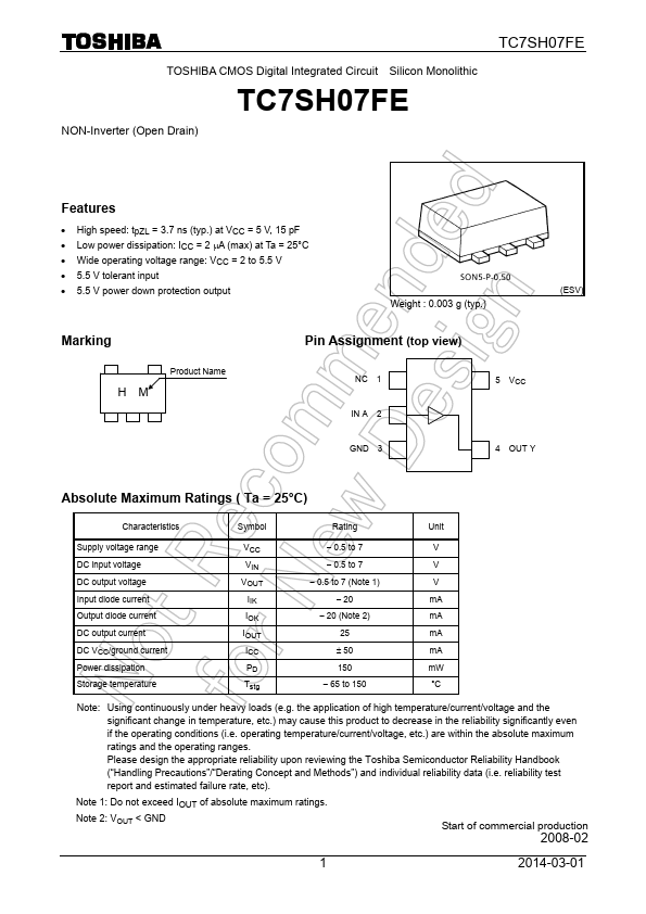
Weight : 0.003 g (typ.)
(ESV)
Marking
HM
Product Name
Pin Assignment (top view)
NC 1
IN A 2
5 VCC
GND 3
4 OUT Y
Absolute Maximum Ratings ( Ta = 25°C)
Characteristics
Symbol
Rating
Unit
Supply voltage range
DC input voltage
DC output voltage
Input diode current
Output diode current
DC output current
DC VCC/ground current
Power dissipation
Storage temperature
VCC
− 0.5 to 7
V
VIN
− 0.5 to 7
V
VOUT
− 0.5 to 7 (Note 1)
V
IIK
− 20
mA
IOK
− 20 (Note 2)
mA
IOUT
25
mA
ICC
± 50
mA
PD
150
mW
Tstg
− 65 to 150
°C
Note: Using continuously under heavy loads (e.g. the application of high temperature/current/voltage and the
significant change in temperature, etc.) may cause this product to decrease in the reliability significantly even
if the operating conditions (i.e. operating temperature/current/voltage, etc.) are within the absolute maximum
ratings and the operating ranges.
Please design the appropriate reliability upon reviewing the Toshiba Semiconductor Reliability Handbook
(“Handling Precautions”/“Derating Concept and Methods”) and individual reliability data (i.e. reliability test
report and estimated failure rate, etc).
Note 1: Do not exceed IOUT of absolute maximum ratings.
Note 2: VOUT < GND
Start of commercial production
2008-02
1
2014-03-01