High speed: tpd = 4.3 ns (typ. ) at VCC = 5 V Low power dissipation: ICC = 2 µA (max) at Ta = 25°C High noise immunity: VNIH = VNIL = 28% VCC (min) 5.5V tolerant input. Wide operating voltage range: VCC (opr) = 2~5.5 V
SON5-P-0.35
Marking
(top view)
H2
Pin Assignment
Weight : 0.001 g (Typ. )
Type Name
IN A 1 GND 2 IN B 3
5 VCC 4 OUT Y
(fSV)
1 2003-08-28
Maximum Ratings (Ta = 25°C)
Characteristics
Supply voltage range DC input voltage DC output voltage Input diode current Output diode cu.
The following content is an automatically extracted verbatim text
from the original manufacturer datasheet and is provided for reference purposes only.
View original datasheet text
TC7SH08FS
TOSHIBA CMOS Digital Integrated Circuit Silicon Monolithic
TC7SH08FS
2-INPUT AND GATE
Features
High speed: tpd = 4.3 ns (typ.) at VCC = 5 V Low power dissipation: ICC = 2 µA (max) at Ta = 25°C High noise immunity: VNIH = VNIL = 28% VCC (min) 5.5V tolerant input. Wide operating voltage range: VCC (opr) = 2~5.5 V
SON5-P-0.35
Marking
(top view)
H2
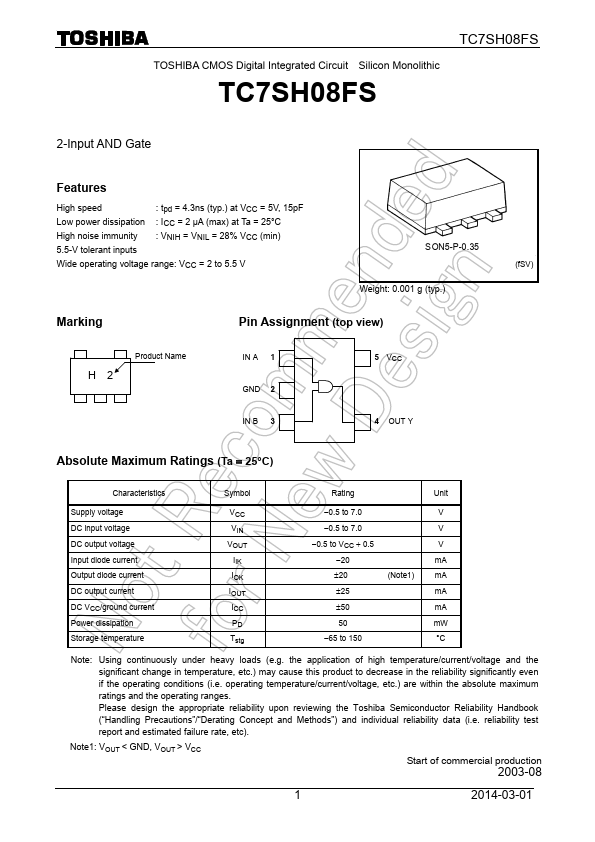
Pin Assignment
Weight : 0.001 g (Typ.)
Type Name
IN A 1 GND 2 IN B 3
5 VCC 4 OUT Y
(fSV)
1 2003-08-28
Maximum Ratings (Ta = 25°C)
Characteristics
Supply voltage range DC input voltage DC output voltage Input diode current Output diode current DC output current DC VCC/ground current Power dissipation Storage temperature
Symbol
VCC VIN VOUT IIK IOK IOUT ICC PD Tstg
Rating
−0.5~7.0 −0.5~7.0 −0.5~VCC + 0.