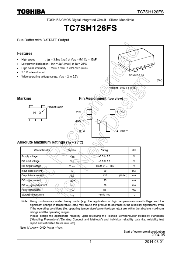
TC7SH126FS
TOSHIBA CMOS Digital Integrated Circuit Silicon Monolithic
TC7SH126FS
Bus Buffer with 3-STATE Output
Features
• High speed
: tpd = 3.8ns (typ.) at VCC = 5V, CL = 15pF
• Low power dissipation : ICC = 2μA (max) at Ta = 25°C
• High noise immunity : VNIH = VNIL = 28% VCC (min)
• 5.5 V tolerant input.
• Wide operating voltage range: VCC = 2 to 5.5V
SON5-P -0.35
Weight : 0.001 g (Typ.)
(fSV)
Marking
HX
Product Name
Pin Assignment (top view)
IN A 1
GND 2
5 VCC
G3
4 OUT Y
Absolute Maximum Ratings (Ta = 25°C)
Characteristics
Symbol
Rating
Unit
Supply voltage
DC input voltage
DC output voltage
Input diode current
Output diode current
DC output current
DC VCC/ground current
Power dissipation
Storage temperature
VCC
VIN
VOUT
IIK
IOK
IOUT
ICC
PD
Tstg
−0.5 to 7.0
−0.5 to 7.0
−0.5 to VCC + 0.5
−20
±20
±25
±50
50
−65 to 150
V
V
V
mA
(Note1) mA
mA
mA
mW
°C
Note: Using continuously under heavy loads (e.g. the application of high temperature/current/voltage and the
significant change in temperature, etc.) may cause this product to decrease in the reliability significantly even
if the operating conditions (i.e. operating temperature/current/voltage, etc.) are within the absolute maximum
ratings and the operating ranges.
Please design the appropriate reliability upon reviewing the Toshiba Semiconductor Reliability Handbook
(“Handling Precautions”/“Derating Concept and Methods”) and individual reliability data (i.e. reliability test
report and estimated failure rate, etc).
Note 1: VOUT < GND, VOUT > VCC
Start of commercial production
2004-05
1
2014-03-01