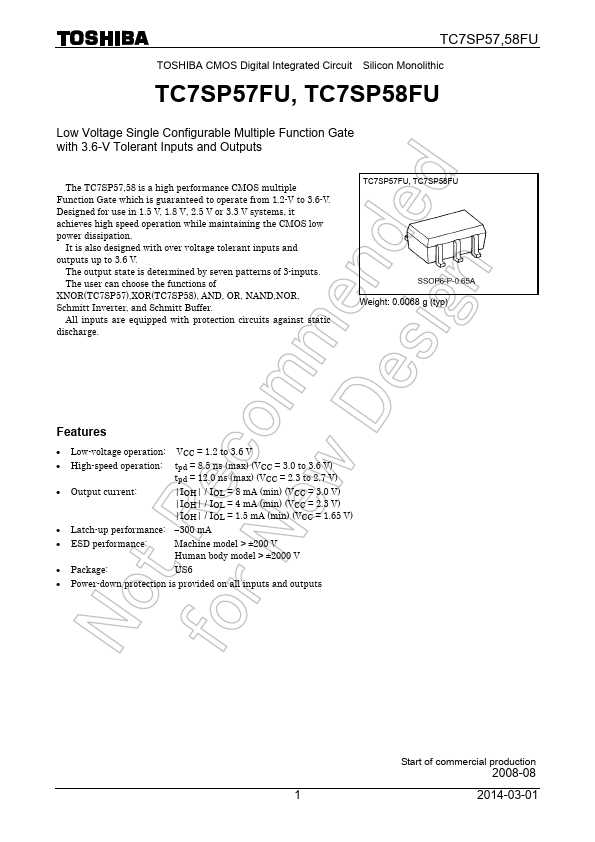
Datasheet4U Logo Datasheet4U.com

TC7SP57FU - Single Configurable Multiple Function Gate

Datasheet Summary

Features

  • Low-voltage operation: VCC = 1.2 to 3.6 V.
  • High-speed operation: tpd = 8.5 ns (max) (VCC = 3.0 to 3.6 V) tpd = 12.0 ns (max) (VCC = 2.3 to 2.7 V).
  • Output current: |IOH| / IOL = 8 mA (min) (VCC = 3.0 V) |IOH| / IOL = 4 mA (min) (VCC = 2.3 V) |IOH| / IOL = 1.5 mA (min) (VCC = 1.65 V).
  • Latch-up performance:.
  • 300 mA.
  • ESD performance: Machine model > ±200 V Human body model > ±2000 V.
  • Package: US6.
  • Power-down protectio.

📥 Download Datasheet

Datasheet preview – TC7SP57FU

Datasheet Details

Part number TC7SP57FU
Manufacturer Toshiba
File Size 258.12 KB
Description Single Configurable Multiple Function Gate
Datasheet download datasheet TC7SP57FU Datasheet
Additional preview pages of the TC7SP57FU datasheet.
Other Datasheets by Toshiba

Full PDF Text Transcription

Click to expand full text
TC7SP57,58FU TOSHIBA CMOS Digital Integrated Circuit Silicon Monolithic TC7SP57FU, TC7SP58FU Low Voltage Single Configurable Multiple Function Gate with 3.6-V Tolerant Inputs and Outputs The TC7SP57,58 is a high performance CMOS multiple Function Gate which is guaranteed to operate from 1.2-V to 3.6-V. Designed for use in 1.5 V, 1.8 V, 2.5 V or 3.3 V systems, it achieves high speed operation while maintaining the CMOS low power dissipation. It is also designed with over voltage tolerant inputs and outputs up to 3.6 V. The output state is determined by seven patterns of 3-inputs. The user can choose the functions of XNOR(TC7SP57),XOR(TC7SP58), AND, OR, NAND,NOR, Schmitt Inverter, and Schmitt Buffer. All inputs are equipped with protection circuits against static discharge.
Published: |