TC7SZ00AFS
TC7SZ00AFS is 2-Input NAND Gate manufactured by Toshiba.
CMOS Digital Integrated Circuits Silicon Monolithic
1. Functional Description
- 2-Input NAND Gate
2. Features
(1) Wide operating temperature range: Topr = -40 to 125 (Note 1) (2) High output current: ±24 m A (min) at VCC = 3.0 V (3) Super high speed operation: tpd = 2.4 ns (typ.) at VCC = 5.0 V, CL = 50 p F (4) Operation voltage range: VCC = 1.65 to 5.5 V (5) 5.5 V tolerant inputs Note 1: For devices with the ordering part number ending in J(T. Topr = -40 to 85 for the other devices.
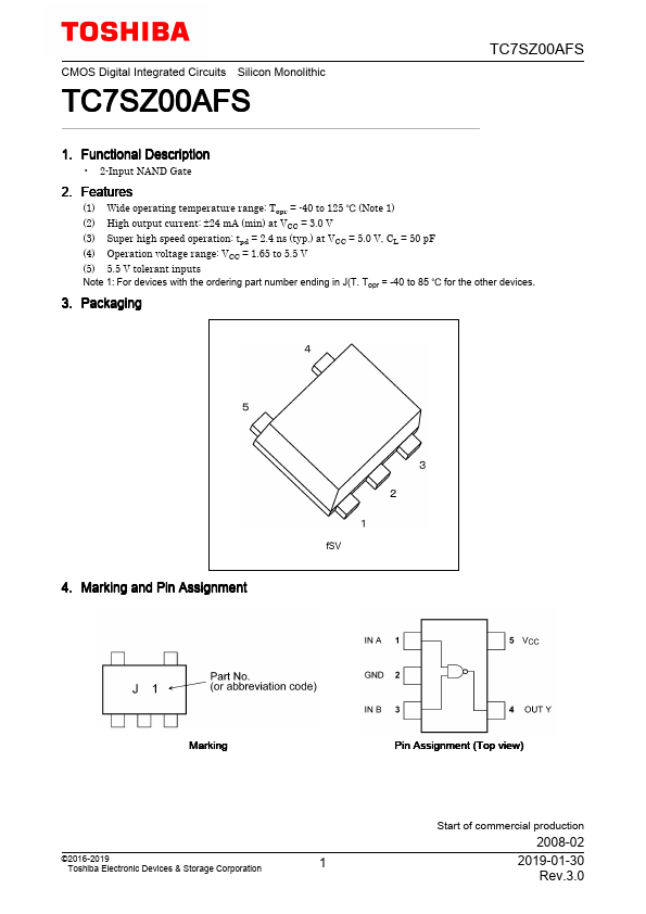
3. Packaging f SV
4. Marking and Pin Assignment
Marking
Pin Assignment (Top view)
©2016-2019 Toshiba Electronic Devices & Storage Corporation
Start of mercial production
2008-02
2019-01-30 Rev.3.0
5. IEC Logic Symbol
6. Truth Table
7....