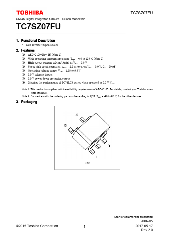
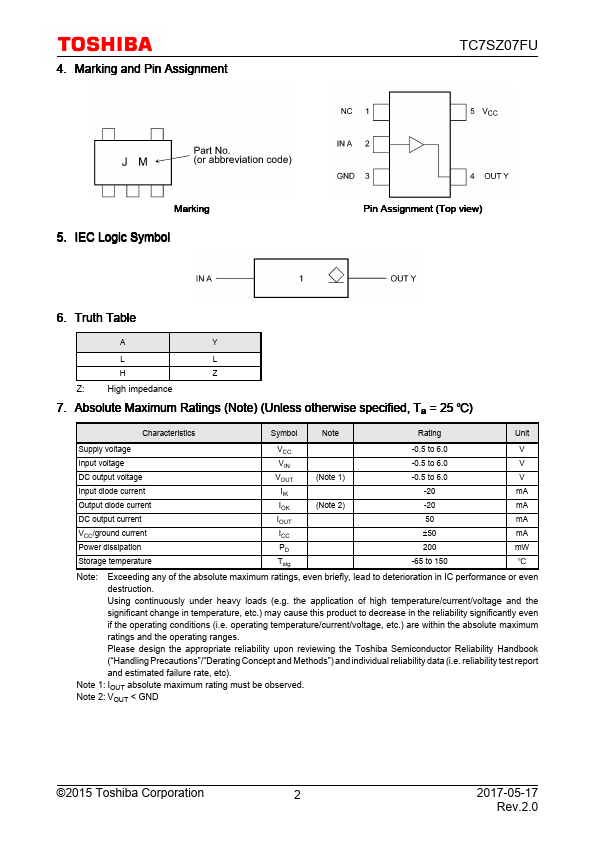
4. Marking and Pin Assignment
TC7SZ07FU
Marking
5. IEC Logic Symbol
Pin Assignment (Top view)
6. Truth Table
A
Y
L
L
H
Z
Z: High impedance
7. Absolute Maximum Ratings (Note) (Unless otherwise specified, Ta = 25 )
Characteristics
Symbol
Note
Rating
Unit
Supply voltage
VCC
-0.5 to 6.0
V
Input voltage
VIN
-0.5 to 6.0
V
DC output voltage
VOUT
(Note 1)
-0.5 to 6.0
V
Input diode current
IIK
-20
mA
Output diode current
IOK
(Note 2)
-20
mA
DC output current
IOUT
50
mA
VCC/ground current
ICC
±50
mA
Power dissipation
PD
200
mW
Storage temperature
Tstg
-65 to 150
Note: Exceeding any of the absolute maximum ratings, even briefly, lead to deterioration in IC performance or even
destruction.
Using continuously under heavy loads (e.g. the application of high temperature/current/voltage and the
significant change in temperature, etc.) may cause this product to decrease in the reliability significantly even
if the operating conditions (i.e. operating temperature/current/voltage, etc.) are within the absolute maximum
ratings and the operating ranges.
Please design the appropriate reliability upon reviewing the Toshiba Semiconductor Reliability Handbook
(“Handling Precautions”/“Derating Concept and Methods”) and individual reliability data (i.e. reliability test report
and estimated failure rate, etc).
Note 1: IOUT absolute maximum rating must be observed.
Note 2: VOUT < GND
©2015 Toshiba Corporation
2
2017-05-17
Rev.2.0