TC7WB66CFK/L8X,TC7WB67CFK/L8X
CMOS Digital Integrated Circuits Silicon Monolithic
TC7WB66CFK,TC7WB66CL8X
TC7WB67CFK,TC7WB67CL8X
1. Functional Description
• Dual SPST Bus Switch
2. General
The TC7WB66CFK/L8X and TC7WB67CFK/L8X are low ON-resistance, high-speed CMOS 2-bit bus switches.
These bus switches allow connections or disconnections to be made with minimal propagation delay while
maintaining Low power dissipation which is the feature of CMOS.
TC7WB66CFK/L8X requires the output enable (OE) input to be set low to place the output into the high impedance
state,whereas the TC7WB67CFK/L8X requires the output enable (OE) input to be set high to place the output
into the high impedance.
These Bus switches consist of P-MOS and N-MOS structure, meaning these devices are suitable for analog signal
transmission.
All inputs are equipped with protector circuits to protect the device from static discharge.
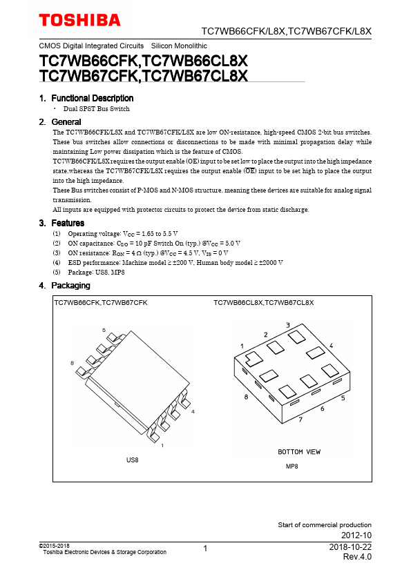
3. Features
(1) Operating voltage: VCC = 1.65 to 5.5 V
(2) ON capacitance: CI/O = 10 pF Switch On (typ.) @VCC = 5.0 V
(3) ON resistance: RON = 4 Ω (typ.) @VCC = 4.5 V, VIS = 0 V
(4) ESD performance: Machine model ≥ ±200 V, Human body model ≥ ±2000 V
(5) Package: US8, MP8
4. Packaging
TC7WB66CFK,TC7WB67CFK
TC7WB66CL8X,TC7WB67CL8X
US8
©2015-2018
Toshiba Electronic Devices & Storage Corporation
1
MP8
Start of commercial production
2012-10
2018-10-22
Rev.4.0