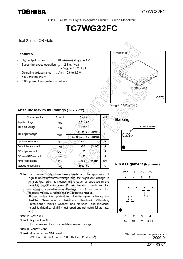
TC7WG32FC
TC7WG32FC is Dual 2-Input OR Gate manufactured by Toshiba.
Features
- High output current
: ±8 m A (min) at VCC = 3 V
- Super high speed operation: tpd = 2.8 ns (typ.) at VCC = 3.3 V, 15p F
- Operating voltage range : VCC = 0.9 to 3.6 V
- 5.5-V tolerant inputs
- 3.6-V power down protection outputs
(CST8)
Absolute Maximum Ratings (Ta = 25°C)
Weight: 0.002 g (typ.)
Characteristics Supply voltage DC input voltage
DC output voltage
Input diode current Output diode current DC output current DC VCC/GND current Power dissipation Storage temperature
Symbol VCC VIN
VOUT
IIK IOK IOUT ICC PD Tstg
Rating
Unit
- 0.5 to 4.6
- 0.5 to 7.0
- 0.5 to 4.6 (Note1) V
- 0.5 to VCC+0.5 (Note2)
- 20 m A
- 20 (Note3) m A
±25 m A
±50 m A
150 (Note4) m W
- 65 to 150
°C
Note: Using continuously under heavy loads (e.g. the application of high temperature/current/voltage and the significant change in temperature, etc.) may cause this product to decrease in the reliability significantly even if the operating conditions (i.e. operating temperature/current/voltage, etc.) are within the absolute maximum ratings and the operating ranges. Please design the appropriate reliability upon reviewing the Toshiba Semiconductor Reliability Handbook (“Handling Precautions”/“Derating Concept and Methods”) and individual reliability data (i.e. reliability test report and estimated failure rate, etc).
Note 1: VCC = 0 V
Note 2: High or Low State. Do not exceed IOUT of absolute maximum ratings.
Note 3: VOUT < GND
Note 4: Mounted on an FR4 board. (25.4 mm × 25.4 mm × 1.6 t, Cu Pad: 11.56 mm2)
Marking
Product name
G32
Pin Assignment (top...