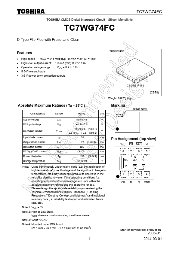
TC7WG74FC
TOSHIBA CMOS Digital Integrated Circuit Silicon Monolithic
TC7WG74FC
D-Type Flip Flop with Preset and Clear
Features
• High-speed fMAX = 246 MHz (typ.) at VCC = 3V, CL = 15pF
• High-level output current: : ±8 mA (min) at VCC = 3V
• Operation voltage range : VCC = 0.9 to 3.6V
• 5.5-V tolerant inputs
• 3.6-V power down protection outputs
TC7WG74FC
Weight: 0.002g (typ.)
(CST8)
Absolute Maximum Ratings ( Ta = 25°C )
Characteristic
Symbol
Rating
Unit
Supply voltage
DC input voltage
DC output voltage
Input diode current
Output diode current
DC output current
DC VCC/GND current
Power dissipation
Storage temperature
VCC
VIN
VOUT
IIK
IOK
IOUT
ICC
PD
Tstg
−0.5 to 4.6
V
−0.5 to 7.0
V
−0.5 to 4.6 (Note 1)
V
−0.5 to VCC + 0.5 (Note 2)
−20
mA
−20 (Note 3) mA
±25
mA
±100
mA
150 (Note 4) mW
−65 to 150
°C
Note:
Using continuously under heavy loads (e.g. the application of
high temperature/current/voltage and the significant change in
temperature, etc.) may cause this product to decrease in the
reliability significantly even if the operating conditions (i.e.
operating temperature/current/voltage, etc.) are within the
absolute maximum ratings and the operating ranges.
Please design the appropriate reliability upon reviewing the
Toshiba Semiconductor Reliability Handbook (“Handling
Precautions”/“Derating Concept and Methods”) and individual
reliability data (i.e. reliability test report and estimated failure
rate, etc).
Note 1: VCC = 0V
Note 2: High or Low State.
IOUT absolute maximum rating must be observed.
Note 3: VOUT < GND
Note 4: Mounted on an FR4 board.
(25.4 mm × 25.4 mm × 1.6 t, Cu Pad: 11.56 mm2)
1
Marking
G74
Product name
Pin Assignment (top view)
VCC PR CLR Q
8765
CK CLR Q
D
PR Q
1234
CK D Q GND
Start of commercial production
2006-01
2014-03-01