TC7WPB9306FK,TC7WPB9307FK
CMOS Digital Integrated Circuits Silicon Monolithic
TC7WPB9306FK,TC7WPB9307FK
1. Functional Description
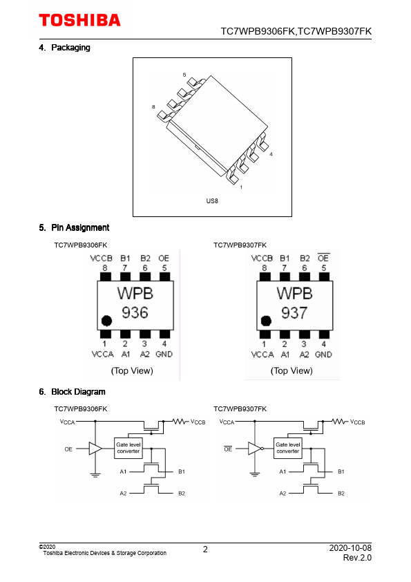
• Low-Voltage, Low-Power 2-Bit Dual-Supply Bus Switch
2. General
The TC7WPB9306FK and TC7WPB9307FK are CMOS 2-bit dual-supply bus switches that can provide an
interface between two nodes at different voltage levels. These devices can be connected to two independent power
supplies. VCCA supports 1.8 V, 2.5 V and 3.3 V power supplies, whereas VCCB supports 2.5 V, 3.3 V and 5.0 V
power supplies.
Bidirectional level-shifting is possible by simply adding external pull-up resistors between the An/Bn data lines
and the VCCA / VCCB supplies. There is no restriction on the relative magnitude of the An and Bn voltages; both
the An and Bn data lines can be pulled up to arbitrary power supplies.
The enable signal can be used to disable the device so that the buses are effectively isolated.
The Output Enable (OE:TC7WPB9306FK, OE:TC7WPB9307FK) input is common for all the 2-bits of the data
lines; thus these device are used as a single 2-bits bus switch. For the TC7WPB9306FK, Output Enable (OE) is
active-High: When OE is High, the switch is on; when Low, the switch is off. For the TC7WPB9307FK, Output
Enable (OE) is active-Low: When OE is Low, the switch is on; when High, the switch is off.
The TC7WPB9306FK and TC7WPB9307FK supports power-down protection at the OE, OE input, with OE, OE
being 5.5 V tolerant.
The channels consist of n-type MOSFETs.
All the inputs provide protection against electrostatic discharge.
3. Features
(1) AEC-Q100 (rev.H) Grade 1 qualified (Note 1)
(2) Wide operating temperature range: Topr = -40 to 125 (Note 2)
(3) Operating voltage: 1.8 V to 2.5 V / 1.8 V to 3.3 V / 1.8 V to 5.0 V / 2.5 V to 3.3 V / 2.5 V to 5.0 V /
3.3 V to 5.0 V bidirectional interface
(4) Operating voltage: VCCA = 1.65 to 5.0 V, VCCB = 2.3 to 5.5 V
(5) Low ON-resistance: RON = 5.0 Ω (typ.) @ VIS = 0 V, IIS = 30 mA, VCCA = 3.0 V, VCCB = 4.5 V
(6) ESD performance: Machine mode ≥ ±200 V, Human body model ≥ ±2000 V
(7) 5.5 V tolerance and power-down protection at the Output Enable input.
(8) Packages: US8
Note 1: This device is compliant with the reliability requirements of AEC-Q100. For details, contact your Toshiba sales
representative.
Note 2: For devices with the ordering part number ending in (CT. Topr = -40 to 85 for the other devices.
©2020
Toshiba Electronic Devices & Storage Corporation
1
Start of commercial production
2020-09
2020-10-08
Rev.2.0