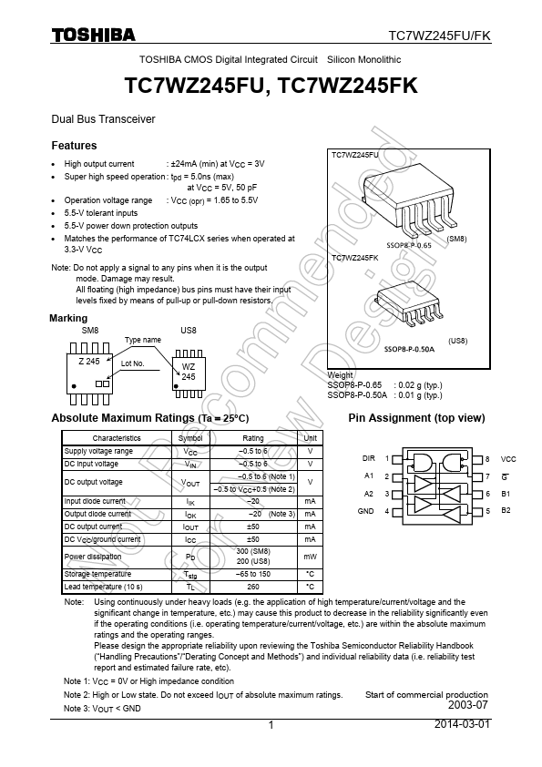
TC7WZ245FU/FK
TOSHIBA CMOS Digital Integrated Circuit Silicon Monolithic
TC7WZ245FU, TC7WZ245FK
Dual Bus Transceiver
Features
• High output current
: ±24mA (min) at VCC = 3V
• Super high speed operation : tpd = 5.0ns (max)
at VCC = 5V, 50 pF
• Operation voltage range : VCC (opr) = 1.65 to 5.5V
• 5.5-V tolerant inputs
• 5.5-V power down protection outputs
• Matches the performance of TC74LCX series when operated at
3.3-V VCC
Note: Do not apply a signal to any pins when it is the output
mode. Damage may result.
All floating (high impedance) bus pins must have their input
levels fixed by means of pull-up or pull-down resistors.
Marking
SM8
Type name
US8
TC7WZ245FU
TC7WZ245FK
(SM8)
(US8)
Z 245
Lot No.
WZ
245
Weight
SSOP8-P-0.65 : 0.02 g (typ.)
SSOP8-P-0.50A : 0.01 g (typ.)
Absolute Maximum Ratings (Ta = 25°C)
Pin Assignment (top view)
Characteristics
Symbol
Rating
Unit
Supply voltage range
DC input voltage
DC output voltage
Input diode current
Output diode current
DC output current
DC VCC/ground current
Power dissipation
VCC
VIN
VOUT
IIK
IOK
IOUT
ICC
PD
−0.5 to 6
V
−0.5 to 6
V
−0.5 to 6 (Note 1)
V
−0.5 to VCC+0.5 (Note 2)
−20
mA
−20 (Note 3) mA
±50
mA
±50
mA
300 (SM8)
mW
200 (US8)
DIR 1
A1 2
A2 3
GND 4
8 VCC
7G
6 B1
5 B2
Storage temperature
Lead temperature (10 s)
Tstg
−65 to 150
°C
TL
260
°C
Note:
Using continuously under heavy loads (e.g. the application of high temperature/current/voltage and the
significant change in temperature, etc.) may cause this product to decrease in the reliability significantly even
if the operating conditions (i.e. operating temperature/current/voltage, etc.) are within the absolute maximum
ratings and the operating ranges.
Please design the appropriate reliability upon reviewing the Toshiba Semiconductor Reliability Handbook
(“Handling Precautions”/“Derating Concept and Methods”) and individual reliability data (i.e. reliability test
report and estimated failure rate, etc).
Note 1: VCC = 0V or High impedance condition
Note 2: High or Low state. Do not exceed IOUT of absolute maximum ratings.
Note 3: VOUT < GND
Start of commercial production
2003-07
1
2014-03-01