TC7WZ38FU
TC7WZ38FU is Dual 2-Input NAND Gate manufactured by Toshiba.
Features
- High output current: 24 m A (min) at VCC = 3 V
- Super high speed operation: tp ZL = 2.2 ns (typ.) at VCC = 5 V, 50 p F
- Operation voltage range: VCC (opr) = 1.65 to 5.5 V
- 5.5-V tolerant inputs
- 5.5-V power down protection outputs
- Matches the performance of TC74LCX series when operated at
3.3-V VCC
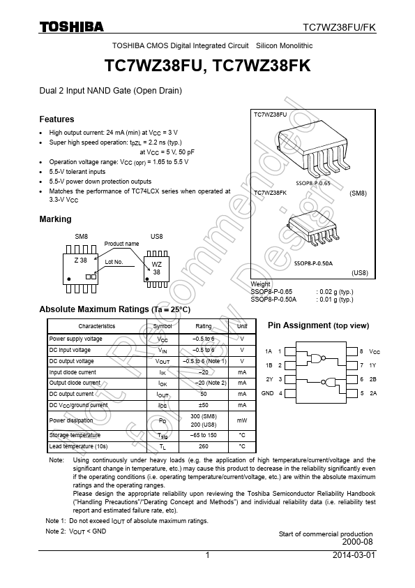
TC7WZ38FU TC7WZ38FK
(SM8)
Marking
SM8
Product name
US8
Z 38
Lot No.
Absolute Maximum Ratings (Ta = 25°C)
Weight SSOP8-P-0.65 SSOP8-P-0.50A
(US8)
: 0.02 g (typ.) : 0.01 g (typ.)
Characteristics
Symbol
Rating
Unit
Pin Assignment (top view)
Power supply voltage DC input voltage DC output voltage Input diode current Output diode current DC output current DC VCC/ground current
Power dissipation
VCC VIN VOUT IIK IOK IOUT ICC
- 0.5 to 6
- 0.5 to 6
- 0.5 to 6 (Note 1) V
- 20 m A
- 20 (Note 2) m A
50 m A
±50 m A
300 (SM8) m...