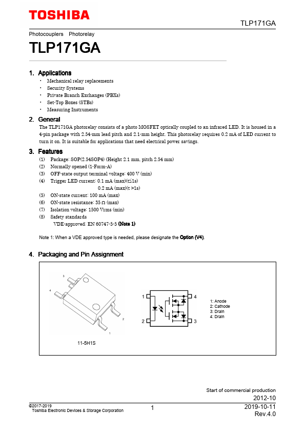
5. Internal Circuit
TLP171GA
6. Absolute Maximum Ratings (Note) (Unless otherwise specified, Ta = 25 )
Characteristics
Symbol Note
Rating
Unit
LED Input forward current
IF
30
mA
Input forward current derating
(Ta ≥ 25 )
∆IF/∆Ta
-0.3
mA/
Input forward current (pulsed)
(100 µs pulse, 100 pps)
IFP
1
A
Input reverse voltage
VR
5
V
Input power dissipation
PD
50
mW
Input power dissipation derating
(Ta ≥ 25 )
∆PD/∆Ta
-0.5
mW/
Junction temperature
Tj
125
Detector OFF-state output terminal voltage
VOFF
400
V
ON-state current
ION
100
mA
ON-state current derating
(Ta ≥ 25 )
∆ION/∆Ta
-1.0
mA/
ON-state current (pulsed)
(t = 100 ms)
IONP
300
mA
Output power dissipation
PO
300
mW
Output power dissipation derating
(Ta ≥ 25 )
∆PO/∆Ta
-3.0
mW/
Junction temperature
Tj
125
Common Storage temperature
Tstg
-55 to 125
Operating temperature
Topr
-40 to 85
Lead soldering temperature
(10 s)
Tsol
260
Isolation voltage
AC, 60 s,
BVS
(Note 1)
R.H. ≤ 60 %, Ta = 25
1500
Vrms
Note: Using continuously under heavy loads (e.g. the application of high temperature/current/voltage and the
significant change in temperature, etc.) may cause this product to decrease in the reliability significantly even
if the operating conditions (i.e. operating temperature/current/voltage, etc.) are within the absolute maximum
ratings.
Please design the appropriate reliability upon reviewing the Toshiba Semiconductor Reliability Handbook
("Handling Precautions"/"Derating Concept and Methods") and individual reliability data (i.e. reliability test
report and estimated failure rate, etc).
Note 1: This device is considered as a two-terminal device: Pins 1 and 2 are shorted together, and pins 3 and 4 are
shorted together.
©2017-2019
Toshiba Electronic Devices & Storage Corporation
2
2019-10-11
Rev.4.0