TLP220GAF
TLP220GAF is Photocoupler Photorelay manufactured by Toshiba.
Photocouplers Photorelay
1. Applications
- Mechanical relay replacements
- Security Systems
- Measuring Instruments
- Factory Automation (FA)
- Amusement Equipment
- Smart Meters
- Electricity Meters
2. General
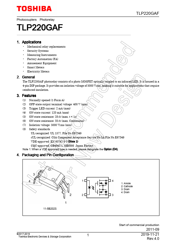
The TLP220GAF photorelay consists of a photo MOSFET optically coupled to an infrared LED. It is housed in a 4-pin DIP package. It provides an isolation voltage of 5000 Vrms, making it suitable for applications that require reinforced insulation.
3. Features
(1) Normally opened (1-Form-A) (2) OFF-state output terminal voltage: 400 V (min) (3) Trigger LED current: 2 mA (max) (4) ON-state current: 120 mA (max) (5) ON-state resistance: 28 Ω (max, t < 1s) (6)...