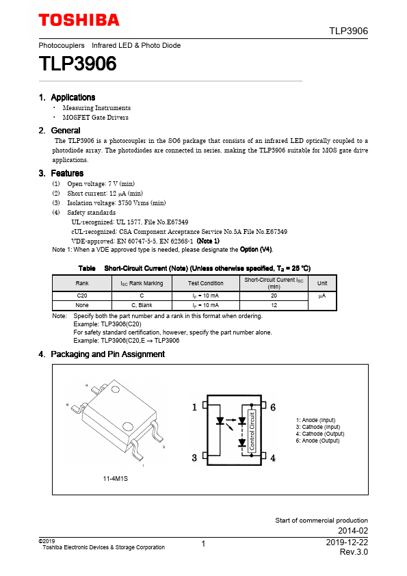
5. Mechanical Parameters
TLP3906
Characteristics
Creepage distances
Clearance
Internal isolation thickness
Min
Unit
5.0
mm
5.0
0.4
6. Absolute Maximum Ratings (Note) (Unless otherwise specified, Ta = 25 )
Characteristics
Symbol
Note
Rating
Unit
LED Input forward current
IF
30
mA
Input forward current
(Ta = 125 )
10
Input forward current derating
(Ta ≥ 100 )
∆IF/∆Ta
-0.8
mA/
Input power dissipation
PD
50
mW
Input power dissipation derating
(Ta ≥ 100 )
∆PD/∆Ta
-1.3
mW/
Input reverse voltage
VR
3
V
Detector Output forward current
IFD
50
µA
Output reverse voltage
VRD
10
V
Output power dissipation
(-40 ≤Ta ≤ 125 )
PO
0.5
mW
Common Operating temperature
Topr
-40 to 125
Storage temperature
Tstg
-55 to 125
Lead soldering temperature
(10 s)
Tsol
260
Isolation voltage
AC, 60 s, R.H. ≤ 60 %
BVS
(Note 1)
3750
Vrms
Note: Using continuously under heavy loads (e.g. the application of high temperature/current/voltage and the
significant change in temperature, etc.) may cause this product to decrease in the reliability significantly even
if the operating conditions (i.e. operating temperature/current/voltage, etc.) are within the absolute maximum
ratings.
Please design the appropriate reliability upon reviewing the Toshiba Semiconductor Reliability Handbook
("Handling Precautions"/"Derating Concept and Methods") and individual reliability data (i.e. reliability test
report and estimated failure rate, etc).
Note 1: This device is considered as a two-terminal device: Pins 1 and 3 are shorted together, and pins 4 and 6 are
shorted together.
7. Recommended Operating Conditions (Note)
Characteristics
Symbol Note Min Typ. Max Unit
Input forward current
IF
12
15
mA
Operating temperature
Topr
-25
100
Note: The recommended operating conditions are given as a design guide necessary to obtain the intended
performance of the device. Each parameter is an independent value. When creating a system design using
this device, the electrical characteristics specified in this data sheet should also be considered.
8. Electrical Characteristics (Unless otherwise specified, Ta = 25 )
Characteristics
LED Input forward voltage
Input reverse current
Input capacitance
Symbol
VF
IR
Ct
Note
Test Condition
IF = 10 mA
VR = 3 V
V = 0 V, f = 1 MHz
Min Typ. Max Unit
1.5 1.65 1.8
V
10
µA
45
pF
©2019
Toshiba Electronic Devices & Storage Corporation
2
2019-12-22
Rev.3.0